C8051F560-TB Silicon Laboratories Inc, C8051F560-TB Datasheet - Page 125
C8051F560-TB
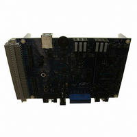
Manufacturer Part Number
C8051F560-TB
Description
BOARD PROTOTYPE W/C8051F560
Manufacturer
Silicon Laboratories Inc
Type
MCUr
Datasheet
1.TOOLSTICK560DC.pdf
(302 pages)
Specifications of C8051F560-TB
Contents
Board
Processor To Be Evaluated
C8051F56x
Processor Series
C8051F56x
Interface Type
USB
Maximum Operating Temperature
+ 125 C
Minimum Operating Temperature
- 40 C
Operating Supply Voltage
1.8 V to 5.25 V
Lead Free Status / RoHS Status
Lead free / RoHS Compliant
For Use With/related Products
C8051F55x, C8051F56x, C8051F57x
For Use With
336-1691 - KIT DEVELOPMENT FOR C8051F560
Lead Free Status / Rohs Status
Lead free / RoHS Compliant
Other names
336-1694


C8051F55x/56x/57x
14.1.3. Flash Write Procedure
Flash bytes are programmed by software with the following sequence:
1. Disable interrupts (recommended).
2. Erase the 512-byte Flash page containing the target location, as described in Section 14.1.2.
3. Set the PSWE bit (register PSCTL).
4. Clear the PSEE bit (register PSCTL).
5. Write the first key code to FLKEY: 0xA5.
6. Write the second key code to FLKEY: 0xF1.
7. Using the MOVX instruction, write a single data byte to the desired location within the 512-byte sector.
8. Clear the PSWE bit.
Steps 5–7 must be repeated for each byte to be written. After Flash writes are complete, PSWE should be
cleared so that MOVX instructions do not target program memory.
14.1.4. Flash Write Optimization
The Flash write procedure includes a block write option to optimize the time to perform consecutive byte
writes. When block write is enabled by setting the CHBLKW bit (CCH0CN.0), writes to two consecutive
bytes in Flash require the same amount of time as a single byte write. This is performed by caching the first
byte that is written to Flash and then committing both bytes to Flash when the second byte is written. When
block writes are enabled, if the second write does not occur, the first data byte written is not actually written
to Flash. Flash bytes with block write enabled are programmed by software with the following sequence:
1. Disable interrupts (recommended).
2. Erase the 512-byte Flash page containing the target location, as described in Section 14.1.2.
3. Set the CHBLKW bit (register CCH0CN).
4. Set the PSWE bit (register PSCTL).
5. Clear the PSEE bit (register PSCTL).
6. Write the first key code to FLKEY: 0xA5.
7. Write the second key code to FLKEY: 0xF1.
8. Using the MOVX instruction, write the first data byte to the desired location within the 512-byte sector.
9. Write the first key code to FLKEY: 0xA5.
10.Write the second key code to FLKEY: 0xF1.
11. Using the MOVX instruction, write the second data byte to the desired location within the 512-byte
sector. The location of the second byte must be the next higher address from the first data byte.
12.Clear the PSWE bit.
13.Clear the CHBLKW bit.
Rev. 1.1
125
Related parts for C8051F560-TB
Image
Part Number
Description
Manufacturer
Datasheet
Request
R

Part Number:
Description:
SMD/C°/SINGLE-ENDED OUTPUT SILICON OSCILLATOR
Manufacturer:
Silicon Laboratories Inc
Part Number:
Description:
Manufacturer:
Silicon Laboratories Inc
Datasheet:
Part Number:
Description:
N/A N/A/SI4010 AES KEYFOB DEMO WITH LCD RX
Manufacturer:
Silicon Laboratories Inc
Datasheet:
Part Number:
Description:
N/A N/A/SI4010 SIMPLIFIED KEY FOB DEMO WITH LED RX
Manufacturer:
Silicon Laboratories Inc
Datasheet:
Part Number:
Description:
N/A/-40 TO 85 OC/EZLINK MODULE; F930/4432 HIGH BAND (REV E/B1)
Manufacturer:
Silicon Laboratories Inc
Part Number:
Description:
EZLink Module; F930/4432 Low Band (rev e/B1)
Manufacturer:
Silicon Laboratories Inc
Part Number:
Description:
I°/4460 10 DBM RADIO TEST CARD 434 MHZ
Manufacturer:
Silicon Laboratories Inc
Part Number:
Description:
I°/4461 14 DBM RADIO TEST CARD 868 MHZ
Manufacturer:
Silicon Laboratories Inc
Part Number:
Description:
I°/4463 20 DBM RFSWITCH RADIO TEST CARD 460 MHZ
Manufacturer:
Silicon Laboratories Inc
Part Number:
Description:
I°/4463 20 DBM RADIO TEST CARD 868 MHZ
Manufacturer:
Silicon Laboratories Inc
Part Number:
Description:
I°/4463 27 DBM RADIO TEST CARD 868 MHZ
Manufacturer:
Silicon Laboratories Inc
Part Number:
Description:
I°/4463 SKYWORKS 30 DBM RADIO TEST CARD 915 MHZ
Manufacturer:
Silicon Laboratories Inc
Part Number:
Description:
N/A N/A/-40 TO 85 OC/4463 RFMD 30 DBM RADIO TEST CARD 915 MHZ
Manufacturer:
Silicon Laboratories Inc
Part Number:
Description:
I°/4463 20 DBM RADIO TEST CARD 169 MHZ
Manufacturer:
Silicon Laboratories Inc