CY8CKIT-020 Cypress Semiconductor Corp, CY8CKIT-020 Datasheet - Page 59
CY8CKIT-020
Manufacturer Part Number
CY8CKIT-020
Description
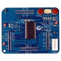
KIT PSOC CY8C28 FAMILY PROCESSOR
Manufacturer
Cypress Semiconductor Corp
Series
PSoC®r
Type
MCUr
Specifications of CY8CKIT-020
Contents
Board, Software and Documentation
Silicon Manufacturer
Cypress
Core Architecture
PSoC
Features
Programmable System-on-chip Design Methodology And Architecture
Kit Contents
PSoC CY8C28 Module, Doc, CD
Silicon Core Number
CY8C28
Silicon Family Name
PSoC
Rohs Compliant
Yes
Lead Free Status / RoHS Status
Lead free / RoHS Compliant
For Use With/related Products
CY8C28 Family
Lead Free Status / Rohs Status
Supplier Unconfirmed
Other names
428-3036


2.1.3.6
2.1.3.7
2.1.3.8
2.1.3.9
2.1.4
CY8CKIT-020 PSoC Development Kit Guide, Doc. # 001-56971 Rev. **
J14 - Wireless Radio Module Power
Header J14 must be jumpered in order to use the Artaflex radio module. Placing a jumper on J14
provides 3.3V power to the P17 module socket. This power is drawn directly from the 3.3V regulator.
R20 - Multipurpose Variable Resistor
The board is equipped with a 10 k thumbwheel variable resistor referenced to ground. The high
side of the resistor is tied to jumper J11. The wiper is tied to a receptacle pin on P14.
J11 - Variable Resistor Power
Header J11 must be jumpered in order to use the variable resistor. Placing a jumper on J11 provides
VDD ANLG power to the high side of the resistor.
SW1 and SW2 - Multipurpose Push Button Switches
The board has two multipurpose mechanical push buttons, SW1 and SW2, that are referenced to
ground. The other sides of the switches are tied to receptacle pins on P14. The switches follow an
inverted logic as they connect ground to receptacle pins on P14 when pressed.
LCD Module
The board has a 2x16 alpha-numeric LCD. I/Os of the module are connected to port two of the PSoC
device and are routed to the processor module socket P2. This LCD is rated for 5V. However, the
I/Os have a level translator inline so that signaling may be as low as 1.8V and still be recognized by
the LCD. The header J12 must be jumpered for the LCD Module to be powered. If J12 is not jum-
pered, it removes power from level translator. If the LCD module is removed, the receptacle pins of
P18 can be used as port 2.
Table 2-3. Connector Pin Assignments - LCD Module Socket
Pin Number
10
11
12
1
2
3
4
5
6
7
8
9
GND
VCC_LCD
VO
RS
R/nW
EN
D0
D1
D2
D3
D4
D5
P18
Board Specifications and Layout
59
Related parts for CY8CKIT-020
Image
Part Number
Description
Manufacturer
Datasheet
Request
R

Part Number:
Description:
KIT DEV FOR PSOC3/5
Manufacturer:
Cypress Semiconductor Corp
Datasheet:

Part Number:
Description:
PSoC1/3/5 Development Kit
Manufacturer:
Cypress Semiconductor Corp
Datasheet:

Part Number:
Description:
KIT DEV PSOC PROC MODULE CY8C38
Manufacturer:
Cypress Semiconductor Corp

Part Number:
Description:
KIT DEV PSOC PROC MODULE CY8C29
Manufacturer:
Cypress Semiconductor Corp

Part Number:
Description:
KIT DEV PSOC ANALOG VOLTMETER
Manufacturer:
Cypress Semiconductor Corp
Datasheet:

Part Number:
Description:
KIT DEV PSOC5 FIRST TOUCH
Manufacturer:
Cypress Semiconductor Corp
Datasheet:

Part Number:
Description:
KIT DEV PSOC3 FIRSTTOUCH STARTER
Manufacturer:
Cypress Semiconductor Corp
Datasheet:
Part Number:
Description:
KIT DEV PROC MODULE PSOC5
Manufacturer:
Cypress Semiconductor Corp
Datasheet:

Part Number:
Description:
KIT PSOC MINIPROG3 PROGRAM DEBUG
Manufacturer:
Cypress Semiconductor Corp
Datasheet:

Part Number:
Description:
DEV KIT PSOC 5 CY8C55
Manufacturer:
Cypress Semiconductor Corp
Datasheet:

Part Number:
Description:
KIT EVAL POWERLINE HIGH VOLT
Manufacturer:
Cypress Semiconductor Corp
Datasheet:

Part Number:
Description:
KIT PSOC FIRST TOUCH
Manufacturer:
Cypress Semiconductor Corp
Datasheet:

Part Number:
Description:
EVAL KIT WORLDTOUR2
Manufacturer:
Cypress Semiconductor Corp
Datasheet:

Part Number:
Description:
KIT UNIVERSAL CAPSENSE CTRLR
Manufacturer:
Cypress Semiconductor Corp
Datasheet: