CY8CKIT-020 Cypress Semiconductor Corp, CY8CKIT-020 Datasheet - Page 54
CY8CKIT-020
Manufacturer Part Number
CY8CKIT-020
Description
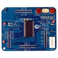
KIT PSOC CY8C28 FAMILY PROCESSOR
Manufacturer
Cypress Semiconductor Corp
Series
PSoC®r
Type
MCUr
Specifications of CY8CKIT-020
Contents
Board, Software and Documentation
Silicon Manufacturer
Cypress
Core Architecture
PSoC
Features
Programmable System-on-chip Design Methodology And Architecture
Kit Contents
PSoC CY8C28 Module, Doc, CD
Silicon Core Number
CY8C28
Silicon Family Name
PSoC
Rohs Compliant
Yes
Lead Free Status / RoHS Status
Lead free / RoHS Compliant
For Use With/related Products
CY8C28 Family
Lead Free Status / Rohs Status
Supplier Unconfirmed
Other names
428-3036


Board Specifications and Layout
2.1.2.5
2.1.2.6
54
Setting a 5V Supply from VBUS
1. Place the jumper on J8 header to select VBUS as the source.
2. Move the VDD select switch to select the 5V.
3. Place the jumper on J6 header to select VDD as source for VDD ANLG.
4. Place the jumper on J7 header to select VDD as source for VDD DIG.
Note 5V operation is not recommended with ES1 Silicon. See the silicon errata for details.
Figure 2-5. Setting a 5V Supply from VBUS
Setting a 3.3V Supply from VBUS
Due to the nature of the PSoC Development Board, powering the system from USB 'VBUS' could
potentially reset other USB devices on the same hub.
By design, the PSoC Development Board is capable of drawing more than 500mA of current during
normal operation, which exceeds USB bus power limits. Additionally, the development board
exceeds inrush current limits due to 'VBUS' capacitance greater than 10uF. As a result, plugging the
PSoC Development Board into a USB hub could potentially cause other devices on the same hub to
reset due to excessive inrush currents. Careful consideration should be taken when powering the
PSoC Development Board from 'VBUS'. In general, it is good practice to plug the PSoC Develop-
ment Board into a host root hub, or a "self-powered" external hub when doing USB development.
Bus powered applications done outside the realm of the PSoC Development Board should comply to
the USB specification for inrush current limits and recommended bulk capacitance on 'VBUS'. See
the
1. Place the jumper on J8 header to select VBUS as the source.
2. Move the VDD select switch to select 3.3V.
3. Place the jumper on J6 header to select VDD as source for VDD ANLG.
4. Place the jumper on J7 header to select VDD as source for VDD DIG.
Universal Serial Bus Specification Revision 2.0
CY8CKIT-020 PSoC Development Kit Guide, Doc. # 001-56971 Rev. **
for more details.
SELECT VDD AS SOURCE
FOR VDD DIG
SELECT VBUS AS SOURCE
MOVE VDD SELECT
SWITCH TO 5V
SELECT VDD AS SOURCE
FOR VDD ANLG
Related parts for CY8CKIT-020
Image
Part Number
Description
Manufacturer
Datasheet
Request
R

Part Number:
Description:
KIT DEV FOR PSOC3/5
Manufacturer:
Cypress Semiconductor Corp
Datasheet:

Part Number:
Description:
PSoC1/3/5 Development Kit
Manufacturer:
Cypress Semiconductor Corp
Datasheet:

Part Number:
Description:
KIT DEV PSOC PROC MODULE CY8C38
Manufacturer:
Cypress Semiconductor Corp

Part Number:
Description:
KIT DEV PSOC PROC MODULE CY8C29
Manufacturer:
Cypress Semiconductor Corp

Part Number:
Description:
KIT DEV PSOC ANALOG VOLTMETER
Manufacturer:
Cypress Semiconductor Corp
Datasheet:

Part Number:
Description:
KIT DEV PSOC5 FIRST TOUCH
Manufacturer:
Cypress Semiconductor Corp
Datasheet:

Part Number:
Description:
KIT DEV PSOC3 FIRSTTOUCH STARTER
Manufacturer:
Cypress Semiconductor Corp
Datasheet:
Part Number:
Description:
KIT DEV PROC MODULE PSOC5
Manufacturer:
Cypress Semiconductor Corp
Datasheet:

Part Number:
Description:
KIT PSOC MINIPROG3 PROGRAM DEBUG
Manufacturer:
Cypress Semiconductor Corp
Datasheet:

Part Number:
Description:
DEV KIT PSOC 5 CY8C55
Manufacturer:
Cypress Semiconductor Corp
Datasheet:

Part Number:
Description:
KIT EVAL POWERLINE HIGH VOLT
Manufacturer:
Cypress Semiconductor Corp
Datasheet:

Part Number:
Description:
KIT PSOC FIRST TOUCH
Manufacturer:
Cypress Semiconductor Corp
Datasheet:

Part Number:
Description:
EVAL KIT WORLDTOUR2
Manufacturer:
Cypress Semiconductor Corp
Datasheet:

Part Number:
Description:
KIT UNIVERSAL CAPSENSE CTRLR
Manufacturer:
Cypress Semiconductor Corp
Datasheet: