EVAL-ADUC832QSZ Analog Devices Inc, EVAL-ADUC832QSZ Datasheet - Page 85
EVAL-ADUC832QSZ
Manufacturer Part Number
EVAL-ADUC832QSZ
Description
KIT DEV FOR ADUC832 QUICK START
Manufacturer
Analog Devices Inc
Series
QuickStart™ Kitr
Type
MCUr
Specifications of EVAL-ADUC832QSZ
Contents
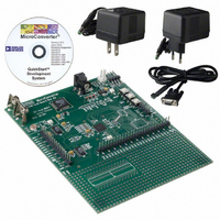
Evaluation Board, Cable, Power Supply, Software and Documentation
Lead Free Status / RoHS Status
Lead free / RoHS Compliant
For Use With/related Products
ADuC832
Lead Free Status / RoHS Status
Compliant, Lead free / RoHS Compliant
Other names
EVAL-ADUC832QS
EVAL-ADUC832QS
EVAL-ADUC832QS


GROUNDING AND BOARD LAYOUT
RECOMMENDATIONS
As with all high resolution data converters, special attention
must be paid to grounding and PCB layout of ADuC832- based
designs to achieve optimum performance from the ADC and
DACs. Although the ADuC832 has separate pins for analog and
digital ground (AGND and DGND), the user must not tie these
to two separate ground planes unless the two ground planes are
connected together very close to the ADuC832, as illustrated in
the simplified example of Figure 93a. In systems where digital
and analog ground planes are connected together at some other
location (at the system’s power supply, for example), they cannot
be connected again near the ADuC832 because a ground loop then
results. In these cases, tie all the ADuC832 AGND and DGND
pins to the analog ground plane, as illustrated in Figure 93b. In
systems with only one ground plane, ensure that the digital and
analog components are physically separated onto separate halves
of the board such that digital return currents do not flow near
analog circuitry and vice versa. The ADuC832 can then be
placed between the digital and analog sections, as illustrated in
Figure 93c.
In all of these scenarios, and in more complicated real-life
applications, keep in mind the flow of current from the supplies
and back to ground. Make sure the return paths for all currents
are as close as possible to the paths the currents traveled to reach
their destinations. For example, do not power components on
the analog side of Figure 93b with DV
return currents from DV
to avoid digital currents flowing under analog circuitry, which
may happen if the user places a noisy digital chip on the left
half of the board in Figure 93c. Whenever possible, avoid large
discontinuities in the ground plane(s) (such as are formed by a
long trace on the same layer), because they force return signals
DD
to flow through AGND. Also, try
DD
because that forces
Rev. A | Page 85 of 92
to travel a longer path. Also, make all connections to the ground
plane directly, with little or no trace separating the pin from its
via to ground.
To connect fast logic signals (rise/fall time < 5 ns) to any of the
ADuC832 digital inputs, add a series resistor to each relevant
line to keep rise and fall times longer than 5 ns at the ADuC832
input pins. A value of 100 Ω or 200 Ω is usually sufficient to
prevent high speed signals from coupling capacitively into the
ADuC832 and affecting the accuracy of ADC conversions.
b.
a.
c.
PLACE ANALOG
PLACE ANALOG
COMPONENTS
COMPONENTS
PLACE ANALOG
COMPONENTS
AGND
HERE
AGND
HERE
Figure 93. System Grounding Schemes
HERE
GND
PLACE DIGITAL
PLACE DIGITAL
COMPONENTS
COMPONENTS
PLACE DIGITAL
COMPONENTS
HERE
HERE
HERE
DGND
DGND
ADuC832
Related parts for EVAL-ADUC832QSZ
Image
Part Number
Description
Manufacturer
Datasheet
Request
R


Part Number:
Description:
BOARD EVAL FOR SI270X-A
Manufacturer:
Silicon Laboratories Inc
Datasheet:

Part Number:
Description:
BUCK CONV REF DESIGN KIT IP1201
Manufacturer:
International Rectifier
Datasheet:
Part Number:
Description:
BOARD DEMO SYNC DUAL BUCK CNVTER
Manufacturer:
International Rectifier
Datasheet:
Part Number:
Description:
BOARD DEMO SYNC BUCK CONVETER
Manufacturer:
International Rectifier
Datasheet:

Part Number:
Description:
EVALBOARD/EB Omnidirectional microphone - Analog
Manufacturer:
Analog Devices
Datasheet:
Part Number:
Description:
EVALBOARD/EB Omnidirectional microphone - Analog
Manufacturer:
Analog Devices
Datasheet:


Part Number:
Description:
BOARD EVAL LED DRIVER LT3756
Manufacturer:
Linear Technology
Datasheet:

Part Number:
Description:
BOARD EVAL FOR AD7741/7742
Manufacturer:
Analog Devices Inc
Datasheet:

Part Number:
Description:
±1.7g Dual-Axis IMEMS Accelerometer Evaluation Board
Manufacturer:
Analog Devices Inc
Datasheet:

Part Number:
Description:
IC MULTIPLIER ANALOG 8-SOIC T/R
Manufacturer:
Analog Devices Inc
Datasheet:

Part Number:
Description:
IC ANALOG MULTIPLIER 8-DIP
Manufacturer:
Analog Devices Inc
Datasheet:
Part Number:
Description:
IC ANALOG MULTIPLIER 8-SOIC
Manufacturer:
Analog Devices Inc
Datasheet:
Part Number:
Description:
IC ANALOG MULTIPLIER 8-DIP
Manufacturer:
Analog Devices Inc
Datasheet: