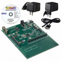
EVAL-ADUC832QSZ Analog Devices Inc, EVAL-ADUC832QSZ Datasheet - Page 40

EVAL-ADUC832QSZ
Manufacturer Part Number
EVAL-ADUC832QSZ
Description
KIT DEV FOR ADUC832 QUICK START
Manufacturer
Analog Devices Inc
Series
QuickStart™ Kitr
Type
MCUr
Specifications of EVAL-ADUC832QSZ
Contents
Evaluation Board, Cable, Power Supply, Software and Documentation
Lead Free Status / RoHS Status
Lead free / RoHS Compliant
For Use With/related Products
ADuC832
Lead Free Status / RoHS Status
Compliant, Lead free / RoHS Compliant
Other names
EVAL-ADUC832QS
EVAL-ADUC832QS
EVAL-ADUC832QS
ADuC832
Table 20. Some Single-Supply Op Amps
Op Amp Model
OP281/OP481
OP191/OP291/OP491
OP196/OP296/OP496
OP183/OP249
OP162/OP262/OP462
AD820/AD822/AD824
AD823
Keep in mind that the ADC’s transfer function is 0 V to V
and any signal range lost to amplifier saturation near ground
impacts dynamic range. Though the op amps in Table 20 are
capable of delivering output signals very closely approaching
ground, no amplifier can deliver signals all the way to ground
when powered by a single supply. Therefore, if a negative supply
is available, consider using it to power the front-end amplifiers.
However, be sure to include the Schottky diodes shown in
Figure 40 (or at least the lower of the two diodes) to protect the
analog input from undervoltage conditions. In summary, use the
circuit of Figure 40 to drive the analog input ADCx pins of the
ADuC832.
VOLTAGE REFERENCE CONNECTIONS
The on-chip 2.5 V band gap voltage reference can be used as
the reference source for the ADC and DACs. To ensure the
accuracy of the voltage reference, the user must decouple the
V
ground with a 0.1 μF capacitor, as shown in Figure 41.
If the internal voltage reference is to be used as a reference for
external circuitry, the C
buffer must be used in this case to ensure that no current is
drawn from the C
that of an internal node within the buffer block, and its voltage
is critical to ADC and DAC accuracy. On the ADuC812, V
the recommended output for the external reference; this can be
used but note that there is a gain error between this reference
and that of the ADC.
REF
pin to ground with a 0.1 μF capacitor, and the C
BUFFER
0.1µF
0.1µF
Figure 41. Decoupling V
REF
C
V
REF
REF
pin itself. The voltage on the C
REF
Characteristics
Micropower
I/O Good up to V
I/O to V
High gain-bandwidth product (GBP)
High GBP, micro package
FET input, low cost
FET input, high GBP
output should be used. However, a
51Ω
BUFFER
DD
, micropower, low cost
REFERENCE
BAND GAP
ADuC832
REF
2.5V
and C
DD
, low cost
REF
REF
REF
pin is
pin to
REF
REF
,
Rev. A | Page 40 of 92
is
The ADuC832 powers up with its internal voltage reference in
the on state. This is available at the V
previously, there is a gain error between this and that of the
ADC. The C
powered up.
If an external voltage reference is preferred, it should be con-
nected to the V
the ADCCON1 SFR must be set to 1 to switch in the external
reference voltage.
To ensure accurate ADC operation, the voltage applied to V
must be between 1 V and AV
input signals are proportional to the power supply (such as
some strain gage applications), it may be desirable to connect
the C
Operation of the ADC or DACs with a reference voltage below
1 V, however, may incur loss of accuracy, eventually resulting in
missing codes or nonmonotonicity. For that reason, do not use
a reference voltage less than 1 V.
To maintain compatibility with the ADuC812, the external
reference can also be connected to the V
Figure 43, to overdrive the internal reference. Note that this
introduces a gain error for the ADC that has to be calibrated
out; thus the previous method is the recommended one for
most users. For this method to work, ADCCON1[6] should be
configured to use the internal reference. The external reference
then overdrives this.
REF
REFERENCE
and V
EXTERNAL
VOLTAGE
V
REF
DD
Figure 42. Using an External Voltage Reference
REF
REF
0.1µF
0.1µF
output becomes available when the ADC is
V
C
REF
REF
pins directly to AV
and C
REF
51Ω
1 = EXTERNAL
0 = INTERNAL
pins as shown in Figure 42. Bit 6 of
DD
ADCCON1[6]
. In situations where analog
REFERENCE
BAND GAP
2.5V
ADuC832
DD
REF
.
pin, but as noted
REF
pin, as shown in
BUFFER
REF


