EVAL-ADUC7026QSPZ Analog Devices Inc, EVAL-ADUC7026QSPZ Datasheet - Page 81
EVAL-ADUC7026QSPZ
Manufacturer Part Number
EVAL-ADUC7026QSPZ
Description
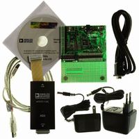
KIT DEV ADUC7026/7027 QUICK PLUS
Manufacturer
Analog Devices Inc
Series
QuickStart™ PLUS Kitr
Type
MCUr
Specifications of EVAL-ADUC7026QSPZ
Contents
Evaluation Board, Power Supply, Cable, Software, Emulator and Documentation
Silicon Manufacturer
Analog Devices
Core Architecture
ARM
Core Sub-architecture
ARM7TDMI
Silicon Core Number
ADuC7026
Rohs Compliant
Yes
Lead Free Status / RoHS Status
Lead free / RoHS Compliant
For Use With/related Products
ADuC7026
Lead Free Status / Rohs Status
Compliant
Available stocks
Company
Part Number
Manufacturer
Quantity
Price
Company:

Part Number:
EVAL-ADUC7026QSPZ
Manufacturer:
Analog Devices Inc
Quantity:
135


XMCFG Register
Name
XMCFG
XMCFG is set to 1 to enable external memory access. This must
be set to 1 before any port pins function as external memory
access pins. The port pins must also be individually enabled via
the GPxCON MMR.
XMxCON Registers
Name
XM0CON
XM1CON
XM2CON
XM3CON
XMxCON are the control registers for each memory region.
They allow the enabling/disabling of a memory region and
control the data bus width of the memory region.
Table 81. XMxCON MMR Bit Descriptions
Bit
1
0
XMxPAR Registers
Name
XM0PAR
XM1PAR
XM2PAR
XM3PAR
Description
Selects Data Bus Width. Set by the user to select a 16-bit
data bus. Cleared by the user to select an 8-bit data bus.
Enables Memory Region. Set by the user to enable memory
region. Cleared by the user to disable the memory region.
Address
0xFFFFF000
Address
0xFFFFF010
0xFFFFF014
0xFFFFF018
0xFFFFF01C
Address
0xFFFFF020
0xFFFFF024
0xFFFFF028
0xFFFFF02C
Default Value
0x00
Default Value
0x00
0x00
0x00
0x00
Default Value
0x70FF
0x70FF
0x70FF
0x70FF
Access
R/W
Access
R/W
R/W
R/W
R/W
Access
R/W
R/W
R/W
R/W
Rev. B | Page 81 of 92
XMxPAR are registers that define the protocol used for
accessing the external memory for each memory region.
Table 82. XMxPAR MMR Bit Descriptions
Bit
15
14:12
11
10
9
8
7:4
3:0
Figure 70, Figure 71, Figure 72, and Figure 73 show the timing
for a read cycle, a read cycle with address hold and bus turn
cycles, a write cycle with address and write hold cycles, and a
write cycle with wait sates, respectively.
ADuC7019/20/21/22/24/25/26/27/28
Description
Enable Byte Write Strobe. This bit is only used for two,
8-bit memory sharing the same memory region. Set by
the user to gate the A0 output with the WS output. This
allows byte write capability without using BHE and BLE
signals. Cleared by user to use BHE and BLE signals.
Number of Wait States on the Address Latch Enable Strobe.
Reserved.
Extra Address Hold Time. Set by the user to disable extra
hold time. Cleared by the user to enable one clock cycle
of hold on the address in read and write.
Extra Bus Transition Time on Read. Set by the user to disable
extra bus transition time. Cleared by the user to enable
one extra clock before and after the read strobe (RS).
Extra Bus Transition Time on Write. Set by the user to disable
extra bus transition time. Cleared by the user to enable
one extra clock before and after the write strobe (WS).
Number of Write Wait States. Select the number of wait
states added to the length of the WS pulse. 0x0 is 1 clock;
0xF is 16 clock cycles (default value).
Number of Read Wait States. Select the number of wait
states added to the length of the RS pulse. 0x0 is 1 clock;
0xF is 16 clock cycles (default value).
Related parts for EVAL-ADUC7026QSPZ
Image
Part Number
Description
Manufacturer
Datasheet
Request
R

Part Number:
Description:
IC, ADJ LDO REG, 1.5V TO 5V 250mA MSOP-8
Manufacturer:
Vishay
Datasheet:

Part Number:
Description:
IC, ADJ LDO REG, 1.5V TO 5V 0.6A 8-TSSOP
Manufacturer:
Vishay
Datasheet:
Part Number:
Description:
IC, ADJ LDO REG, 1.5V TO 5V 250mA MSOP-8
Manufacturer:
Vishay
Datasheet:

Part Number:
Description:
IC ADJ LDO REG 1.5V TO 5V 150mA 5-SOT-23
Manufacturer:
Vishay
Datasheet:

Part Number:
Description:
BOARD EVAL AS1324-AD
Manufacturer:
austriamicrosystems
Datasheet:
Part Number:
Description:
IC, ADJ LDO REG, 1.5V TO 5V 0.6A 8-TSSOP
Manufacturer:
Vishay
Datasheet:

Part Number:
Description:
IC, ADJ LDO REG, 1.5V TO 5V, 0.3A, MSOP8
Manufacturer:
Vishay
Datasheet:
Part Number:
Description:
IC, ADJ LDO REG, 1.5V TO 5V, 0.3A, MSOP8
Manufacturer:
Vishay
Datasheet:
Part Number:
Description:
IC, ADJ LDO REG 1.215V TO 5V 0.3A MSOP-8
Manufacturer:
Vishay
Datasheet:
Part Number:
Description:
IC, ADJ LDO REG 1.215V TO 5V 0.3A MSOP-8
Manufacturer:
Vishay
Datasheet:

Part Number:
Description:
±1.7g Dual-Axis IMEMS Accelerometer Evaluation Board
Manufacturer:
Analog Devices Inc
Datasheet:

Part Number:
Description:
IC MULTIPLIER ANALOG 8-SOIC T/R
Manufacturer:
Analog Devices Inc
Datasheet:

Part Number:
Description:
IC ANALOG MULTIPLIER 8-DIP
Manufacturer:
Analog Devices Inc
Datasheet:
Part Number:
Description:
IC ANALOG MULTIPLIER 8-SOIC
Manufacturer:
Analog Devices Inc
Datasheet:
Part Number:
Description:
IC ANALOG MULTIPLIER 8-DIP
Manufacturer:
Analog Devices Inc
Datasheet: