EVAL-ADUC7026QSPZ Analog Devices Inc, EVAL-ADUC7026QSPZ Datasheet - Page 50
EVAL-ADUC7026QSPZ
Manufacturer Part Number
EVAL-ADUC7026QSPZ
Description
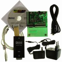
KIT DEV ADUC7026/7027 QUICK PLUS
Manufacturer
Analog Devices Inc
Series
QuickStart™ PLUS Kitr
Type
MCUr
Specifications of EVAL-ADUC7026QSPZ
Contents
Evaluation Board, Power Supply, Cable, Software, Emulator and Documentation
Silicon Manufacturer
Analog Devices
Core Architecture
ARM
Core Sub-architecture
ARM7TDMI
Silicon Core Number
ADuC7026
Rohs Compliant
Yes
Lead Free Status / RoHS Status
Lead free / RoHS Compliant
For Use With/related Products
ADuC7026
Lead Free Status / Rohs Status
Compliant
Available stocks
Company
Part Number
Manufacturer
Quantity
Price
Company:

Part Number:
EVAL-ADUC7026QSPZ
Manufacturer:
Analog Devices Inc
Quantity:
135


ADuC7019/20/21/22/24/25/26/27/28
Linearity degradation near ground and V
ration of the output amplifier, and a general representation of its
effects (neglecting offset and gain error) is illustrated in Figure 53.
The dotted line in Figure 53 indicates the ideal transfer function,
and the solid line represents what the transfer function may
look like with endpoint nonlinearities due to saturation of the
output amplifier. Note that Figure 53 represents a transfer function
in 0-to-AV
(with V
similar. However, the upper portion of the transfer function
follows the ideal line right to the end (V
showing no signs of endpoint linearity errors.
The endpoint nonlinearities conceptually illustrated in
Figure 53 get worse as a function of output loading. Most
of the ADuC7019/20/21/22/24/25/26/27/28 data sheet
specifications assume a 5 kΩ resistive load to ground at the
DAC output. As the output is forced to source or sink more
current, the nonlinear regions at the top or bottom (respectively)
of Figure 53 become larger. With larger current demands, this
can significantly limit output voltage swing.
POWER SUPPLY MONITOR
The power supply monitor regulates the IOV
ADuC7019/20/21/22/24/25/26/27/28. It indicates when the
IOV
The monitor function is controlled via the PSMCON register.
If enabled in the IRQEN or FIQEN register, the monitor
interrupts the core using the PSMI bit in the PSMCON MMR.
This bit is immediately cleared once CMP goes high.
This monitor function allows the user to save working registers
to avoid possible data loss due to low supply or brown-out
conditions. It also ensures that normal code execution does not
resume until a safe supply level has been established.
PSMCON Register
Name
PSMCON
DD
Figure 53. Endpoint Nonlinearities Due to Amplifier Saturation
AV
supply pin drops below one of two supply trip points.
REF
DD
< AV
DD
– 100mV
100mV
mode only. In 0-to-V
AV
Address
0xFFFF0440
DD
DD
or DAC
0x00000000
REF
< AV
Default Value
0x0008
REF
DD
), the lower nonlinearity is
REF
or 0-to-DAC
in this case, not AV
DD
is caused by satu-
DD
0x0FFF0000
supply on the
REF
modes
Access
R/W
DD
Rev. B | Page 50 of 92
),
Table 29. PSMCON MMR Bit Descriptions
Bit
3
2
1
0
COMPARATOR
The ADuC7019/20/21/22/24/25/26/27/28 integrate voltage
comparators. The positive input is multiplexed with ADC2 and
the negative input has two options: ADC3 or DAC0. The output
of the comparator can be configured to generate a system
interrupt, be routed directly to the programmable logic array,
start an ADC conversion, or be on an external pin, CMP
shown in Figure 54.
Note that because the ADuC7022, ADuC7025, and ADu7027
parts do not support a DAC0 output, it is not possible to use
DAC0 as a comparator input on these parts.
Hysteresis
Figure 55 shows how the input offset voltage and hysteresis
terms are defined. Input offset voltage (V
between the center of the hysteresis range and the ground level.
This can either be positive or negative. The hysteresis voltage
(V
H
) is ½ the width of the hysteresis range.
Name
CMP
TP
PSMEN
PSMI
P0.0/CMP
ADC2/CMP0
ADC3/CMP1
Figure 55. Comparator Hysteresis Transfer Function
CMP
OUT
Description
Comparator Bit. This is a read-only bit that
directly reflects the state of the comparator.
Read 1 indicates the IOV
selected trip point, or the PSM is in power-down
mode. Read 0 indicates the IOV
below its selected trip point. This bit should be
set before leaving the interrupt service routine.
Trip Point Selection Bits. 0 = 2.79 V, 1 = 3.07 V.
Power Supply Monitor Enable Bit. Set to 1 to
enable the power supply monitor circuit. Clear to
0 to disable the power supply monitor circuit.
Power Supply Monitor Interrupt Bit. This bit is set
high by the MicroConverter once CMP goes low,
indicating low I/O supply. The PSMI bit can be
used to interrupt the processor. Once CMP
returns high, the PSMI bit can be cleared by
writing a 1 to this location. A 0 write has no
effect. There is no timeout delay; PSMI can be
immediately cleared once CMP goes high.
OUT
DAC0
V
Figure 54. Comparator
OS
V
H
MUX
V
H
DD
OS
supply is above its
COMP0
) is the difference
MUX
DD
supply is
IRQ
OUT
, as
Related parts for EVAL-ADUC7026QSPZ
Image
Part Number
Description
Manufacturer
Datasheet
Request
R

Part Number:
Description:
IC, ADJ LDO REG, 1.5V TO 5V 250mA MSOP-8
Manufacturer:
Vishay
Datasheet:

Part Number:
Description:
IC, ADJ LDO REG, 1.5V TO 5V 0.6A 8-TSSOP
Manufacturer:
Vishay
Datasheet:
Part Number:
Description:
IC, ADJ LDO REG, 1.5V TO 5V 250mA MSOP-8
Manufacturer:
Vishay
Datasheet:

Part Number:
Description:
IC ADJ LDO REG 1.5V TO 5V 150mA 5-SOT-23
Manufacturer:
Vishay
Datasheet:

Part Number:
Description:
BOARD EVAL AS1324-AD
Manufacturer:
austriamicrosystems
Datasheet:
Part Number:
Description:
IC, ADJ LDO REG, 1.5V TO 5V 0.6A 8-TSSOP
Manufacturer:
Vishay
Datasheet:

Part Number:
Description:
IC, ADJ LDO REG, 1.5V TO 5V, 0.3A, MSOP8
Manufacturer:
Vishay
Datasheet:
Part Number:
Description:
IC, ADJ LDO REG, 1.5V TO 5V, 0.3A, MSOP8
Manufacturer:
Vishay
Datasheet:
Part Number:
Description:
IC, ADJ LDO REG 1.215V TO 5V 0.3A MSOP-8
Manufacturer:
Vishay
Datasheet:
Part Number:
Description:
IC, ADJ LDO REG 1.215V TO 5V 0.3A MSOP-8
Manufacturer:
Vishay
Datasheet:

Part Number:
Description:
±1.7g Dual-Axis IMEMS Accelerometer Evaluation Board
Manufacturer:
Analog Devices Inc
Datasheet:

Part Number:
Description:
IC MULTIPLIER ANALOG 8-SOIC T/R
Manufacturer:
Analog Devices Inc
Datasheet:

Part Number:
Description:
IC ANALOG MULTIPLIER 8-DIP
Manufacturer:
Analog Devices Inc
Datasheet:
Part Number:
Description:
IC ANALOG MULTIPLIER 8-SOIC
Manufacturer:
Analog Devices Inc
Datasheet:
Part Number:
Description:
IC ANALOG MULTIPLIER 8-DIP
Manufacturer:
Analog Devices Inc
Datasheet: