EVAL-ADUC7026QSPZ Analog Devices Inc, EVAL-ADUC7026QSPZ Datasheet - Page 80
EVAL-ADUC7026QSPZ
Manufacturer Part Number
EVAL-ADUC7026QSPZ
Description
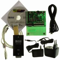
KIT DEV ADUC7026/7027 QUICK PLUS
Manufacturer
Analog Devices Inc
Series
QuickStart™ PLUS Kitr
Type
MCUr
Specifications of EVAL-ADUC7026QSPZ
Contents
Evaluation Board, Power Supply, Cable, Software, Emulator and Documentation
Silicon Manufacturer
Analog Devices
Core Architecture
ARM
Core Sub-architecture
ARM7TDMI
Silicon Core Number
ADuC7026
Rohs Compliant
Yes
Lead Free Status / RoHS Status
Lead free / RoHS Compliant
For Use With/related Products
ADuC7026
Lead Free Status / Rohs Status
Compliant
Available stocks
Company
Part Number
Manufacturer
Quantity
Price
Company:

Part Number:
EVAL-ADUC7026QSPZ
Manufacturer:
Analog Devices Inc
Quantity:
135


ADuC7019/20/21/22/24/25/26/27/28
Secure Clear Bit (Watchdog Mode Only)
The secure clear bit is provided for a higher level of protection.
When set, a specific sequential value must be written to T3CLRI
to avoid a watchdog reset. The value is a sequence generated
by the 8-bit linear feedback shift register (LFSR) polynomial =
X8 + X6 + X5 + X + 1 as shown in Figure 68.
CLOCK
The initial value or seed is written to T3CLRI before entering
watchdog mode. After entering watchdog mode, a write to
T3CLRI must match this expected value. If it matches, the LFSR
is advanced to the next state when the counter reload happens.
If it fails to match the expected state, a reset is immediately
generated, even if the count has not yet expired.
The value 0x00 should not be used as an initial seed due to the
properties of the polynomial. The value 0x00 is always
guaranteed to force an immediate reset. The value of the LFSR
cannot be read; it must be tracked/generated in software.
Example of a sequence:
1.
2.
3.
4.
5.
EXTERNAL MEMORY INTERFACING
The ADuC7026 and ADuC7027 are the only models in their
series that feature an external memory interface. The external
memory interface requires a larger number of pins. This is why
it is only available on larger pin count packages. The XMCFG
MMR must be set to 1 to use the external port.
Although 32-bit addresses are supported internally, only the
lower 16 bits of the address are on external pins.
The memory interface can address up to four 128 kB of
asynchronous memory (SRAM or/and EEPROM).
The pins required for interfacing to an external memory are
shown in Table 79.
Q
Enter initial seed, 0xAA, in T3CLRI before starting Timer3
in watchdog mode.
Enter 0xAA in T3CLRI; Timer3 is reloaded.
Enter 0x37 in T3CLRI; Timer3 is reloaded.
Enter 0x6E in T3CLRI; Timer3 is reloaded.
Enter 0x66. 0xDC was expected; the watchdog resets the chip.
7
D
Q
6
D
Q
5
D
Figure 68. 8-Bit LFSR
Q
4
D
Q
3
D
Q
2
D
Q
1
D
Q
0
Rev. B | Page 80 of 92
D
Table 79. External Memory Interfacing Pins
Pin
AD[15:0]
A16
MS[3:0]
WS
RS
AE
BHE, BLE
There are four external memory regions available as described
in Table 80. Associated with each region are the MS[3:0] pins.
These signals allow access to the particular region of external
memory. The size of each memory region can be 128 kB maxi-
mum, 64 k × 16 or 128 k × 8. To access 128 k with an 8-bit
memory, an extra address line (A16) is provided. (See the example
in Figure 69). The four regions are configured independently.
Table 80. Memory Regions
Address Start
0x10000000
0x20000000
0x30000000
0x40000000
Each external memory region can be controlled through three
MMRs: XMCFG, XMxCON, and XMxPAR.
ADuC7026/
ADuC7027
AD15:AD0
Figure 69. Interfacing to External EEPROM/RAM
Function
Address/Data Bus.
Extended Addressing for 8-Bit Memory Only.
Memory Select.
Write Strobe.
Read Strobe.
Address Latch Enable.
Byte Write Capability.
MS0
MS1
A16
WS
AE
RS
Address End
0x1000FFFF
0x2000FFFF
0x3000FFFF
0x4000FFFF
LATCH
Contents
External Memory 0
External Memory 1
External Memory 2
External Memory 3
D0:D15
A0:A15
CS
WE
OE
D0:D7
A16
A0:A15
CS
WE
OE
64k × 16-BIT
128k × 8-BIT
EEPROM
RAM
Related parts for EVAL-ADUC7026QSPZ
Image
Part Number
Description
Manufacturer
Datasheet
Request
R

Part Number:
Description:
IC, ADJ LDO REG, 1.5V TO 5V 250mA MSOP-8
Manufacturer:
Vishay
Datasheet:

Part Number:
Description:
IC, ADJ LDO REG, 1.5V TO 5V 0.6A 8-TSSOP
Manufacturer:
Vishay
Datasheet:
Part Number:
Description:
IC, ADJ LDO REG, 1.5V TO 5V 250mA MSOP-8
Manufacturer:
Vishay
Datasheet:

Part Number:
Description:
IC ADJ LDO REG 1.5V TO 5V 150mA 5-SOT-23
Manufacturer:
Vishay
Datasheet:

Part Number:
Description:
BOARD EVAL AS1324-AD
Manufacturer:
austriamicrosystems
Datasheet:
Part Number:
Description:
IC, ADJ LDO REG, 1.5V TO 5V 0.6A 8-TSSOP
Manufacturer:
Vishay
Datasheet:

Part Number:
Description:
IC, ADJ LDO REG, 1.5V TO 5V, 0.3A, MSOP8
Manufacturer:
Vishay
Datasheet:
Part Number:
Description:
IC, ADJ LDO REG, 1.5V TO 5V, 0.3A, MSOP8
Manufacturer:
Vishay
Datasheet:
Part Number:
Description:
IC, ADJ LDO REG 1.215V TO 5V 0.3A MSOP-8
Manufacturer:
Vishay
Datasheet:
Part Number:
Description:
IC, ADJ LDO REG 1.215V TO 5V 0.3A MSOP-8
Manufacturer:
Vishay
Datasheet:

Part Number:
Description:
±1.7g Dual-Axis IMEMS Accelerometer Evaluation Board
Manufacturer:
Analog Devices Inc
Datasheet:

Part Number:
Description:
IC MULTIPLIER ANALOG 8-SOIC T/R
Manufacturer:
Analog Devices Inc
Datasheet:

Part Number:
Description:
IC ANALOG MULTIPLIER 8-DIP
Manufacturer:
Analog Devices Inc
Datasheet:
Part Number:
Description:
IC ANALOG MULTIPLIER 8-SOIC
Manufacturer:
Analog Devices Inc
Datasheet:
Part Number:
Description:
IC ANALOG MULTIPLIER 8-DIP
Manufacturer:
Analog Devices Inc
Datasheet: