EVAL-ADUC7026QSPZ Analog Devices Inc, EVAL-ADUC7026QSPZ Datasheet - Page 66
EVAL-ADUC7026QSPZ
Manufacturer Part Number
EVAL-ADUC7026QSPZ
Description
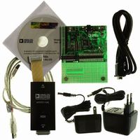
KIT DEV ADUC7026/7027 QUICK PLUS
Manufacturer
Analog Devices Inc
Series
QuickStart™ PLUS Kitr
Type
MCUr
Specifications of EVAL-ADUC7026QSPZ
Contents
Evaluation Board, Power Supply, Cable, Software, Emulator and Documentation
Silicon Manufacturer
Analog Devices
Core Architecture
ARM
Core Sub-architecture
ARM7TDMI
Silicon Core Number
ADuC7026
Rohs Compliant
Yes
Lead Free Status / RoHS Status
Lead free / RoHS Compliant
For Use With/related Products
ADuC7026
Lead Free Status / Rohs Status
Compliant
Available stocks
Company
Part Number
Manufacturer
Quantity
Price
Company:

Part Number:
EVAL-ADUC7026QSPZ
Manufacturer:
Analog Devices Inc
Quantity:
135


ADuC7019/20/21/22/24/25/26/27/28
Table 57. COMIID1 MMR Bit Descriptions
Bit 3:1
Status
Bits
000
110
101
011
010
001
000
Note that to receive a network address interrupt, the slave must
ensure that Bit 0 of COMIEN0 (enable receive buffer full interrupt)
is set to 1.
COMADR Register
Name
COMADR
COMADR is an 8-bit, read/write network address register that
holds the address checked for by the network addressable
UART. Upon receiving this address, the device interrupts the
processor and/or sets the appropriate status bit in COMIID1.
SERIAL PERIPHERAL INTERFACE
The ADuC7019/20/21/22/24/25/26/27/28 integrate a complete
hardware serial peripheral interface (SPI) on-chip. SPI is an indus-
try standard, synchronous serial interface that allows eight bits
of data to be synchronously transmitted and simultaneously
received, that is, full duplex up to a maximum bit rate of 3.48 Mb
as shown in Table 58. The SPI interface is not operational with core
clock divider (CD) bits. POWCON[2:0] = 6 or 7 in master mode.
The SPI port can be configured for master or slave operation
and typically consists of four pins: MISO, MOSI, SCL, and CS .
MISO (Master In, Slave Out) Pin
The MISO pin is configured as an input line in master mode
and an output line in slave mode. The MISO line on the master
(data in) should be connected to the MISO line in the slave
device (data out). The data is transferred as byte wide (8-bit)
serial data, MSB first.
MOSI (Master Out, Slave In) Pin
The MOSI pin is configured as an output line in master mode
and an input line in slave mode. The MOSI line on the master
(data out) should be connected to the MOSI line in the slave
device (data in). The data is transferred as byte wide (8-bit)
serial data, MSB first.
Bit 0
NINT
1
0
0
0
0
0
0
Address
0xFFFF0728
Priority
–
2
3
1
2
3
4
Definition
No Interrupt.
Matching
Network Address.
Address
Transmitted,
Buffer Empty.
Receive Line
Status Interrupt.
Receive Buffer Full
Interrupt.
Transmit Buffer
Empty Interrupt.
Modem Status
Interrupt.
Default Value
0xAA
Clearing
Operation
–
Read COMRX.
Write data to
COMTX or
read COMIID0.
Read
COMSTA0.
Read COMRX.
Write data to
COMTX or
read COMIID0.
Read
COMSTA1.
Access
R/W
Rev. B | Page 66 of 92
SCL (Serial Clock I/O) Pin
The master serial clock (SCL) is used to synchronize the data
being transmitted and received through the MOSI SCL period.
Therefore, a byte is transmitted/received after eight SCL periods.
The SCL pin is configured as an output in master mode and as
an input in slave mode.
In master mode, polarity and phase of the clock are controlled
by the SPICON register, and the bit rate is defined in the
SPIDIV register as follows:
The maximum speed of the SPI clock is dependent on the clock
divider bits and is summarized in Table 58.
Table 58. SPI Speed vs. Clock Divider Bits in Master Mode
CD Bits
SPIDIV in hex
SPI speed
in MHz
In slave mode, the SPICON register must be configured with
the phase and polarity of the expected input clock. The slave
accepts data from an external master up to 10.4 Mb at CD = 0.
The formula to determine the maximum speed is as follows:
In both master and slave modes, data is transmitted on one edge
of the SCL signal and sampled on the other. Therefore, it is
important that the polarity and phase are configured the same
for the master and slave devices.
Chip Select ( CS Input) Pin
In SPI slave mode, a transfer is initiated by the assertion of CS ,
which is an active low input signal. The SPI port then transmits
and receives 8-bit data until the transfer is concluded by
deassertion of CS . In slave mode, CS is always an input.
SPI Registers
The following MMR registers are used to control the SPI
interface: SPISTA, SPIRX, SPITX, SPIDIV, and SPICON.
SPISTA Register
Name
SPISTA
SPISTA is an 8-bit read-only status register. Only Bit 1 or Bit 4
of this register generates an interrupt. Bit 6 of the SPICON
register determines which bit generates the interrupt.
f
f
SERIAL
SERIAL
CLOCK
CLOCK
Address
0xFFFF0A00
0
0x05
3.482
=
=
2
f
HCLK
×
4
1 (
1
0x0B
1.741
+
f
UCLK
SPIDIV
2
0x17
0.870
Default Value
0x00
)
3
0x2F
0.435
4
0x5F
0.218
Access
R/W
5
0xBF
0.109
Related parts for EVAL-ADUC7026QSPZ
Image
Part Number
Description
Manufacturer
Datasheet
Request
R

Part Number:
Description:
IC, ADJ LDO REG, 1.5V TO 5V 250mA MSOP-8
Manufacturer:
Vishay
Datasheet:

Part Number:
Description:
IC, ADJ LDO REG, 1.5V TO 5V 0.6A 8-TSSOP
Manufacturer:
Vishay
Datasheet:
Part Number:
Description:
IC, ADJ LDO REG, 1.5V TO 5V 250mA MSOP-8
Manufacturer:
Vishay
Datasheet:

Part Number:
Description:
IC ADJ LDO REG 1.5V TO 5V 150mA 5-SOT-23
Manufacturer:
Vishay
Datasheet:

Part Number:
Description:
BOARD EVAL AS1324-AD
Manufacturer:
austriamicrosystems
Datasheet:
Part Number:
Description:
IC, ADJ LDO REG, 1.5V TO 5V 0.6A 8-TSSOP
Manufacturer:
Vishay
Datasheet:

Part Number:
Description:
IC, ADJ LDO REG, 1.5V TO 5V, 0.3A, MSOP8
Manufacturer:
Vishay
Datasheet:
Part Number:
Description:
IC, ADJ LDO REG, 1.5V TO 5V, 0.3A, MSOP8
Manufacturer:
Vishay
Datasheet:
Part Number:
Description:
IC, ADJ LDO REG 1.215V TO 5V 0.3A MSOP-8
Manufacturer:
Vishay
Datasheet:
Part Number:
Description:
IC, ADJ LDO REG 1.215V TO 5V 0.3A MSOP-8
Manufacturer:
Vishay
Datasheet:

Part Number:
Description:
±1.7g Dual-Axis IMEMS Accelerometer Evaluation Board
Manufacturer:
Analog Devices Inc
Datasheet:

Part Number:
Description:
IC MULTIPLIER ANALOG 8-SOIC T/R
Manufacturer:
Analog Devices Inc
Datasheet:

Part Number:
Description:
IC ANALOG MULTIPLIER 8-DIP
Manufacturer:
Analog Devices Inc
Datasheet:
Part Number:
Description:
IC ANALOG MULTIPLIER 8-SOIC
Manufacturer:
Analog Devices Inc
Datasheet:
Part Number:
Description:
IC ANALOG MULTIPLIER 8-DIP
Manufacturer:
Analog Devices Inc
Datasheet: