EVAL-ADUC7026QSPZ Analog Devices Inc, EVAL-ADUC7026QSPZ Datasheet - Page 18
EVAL-ADUC7026QSPZ
Manufacturer Part Number
EVAL-ADUC7026QSPZ
Description
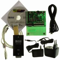
KIT DEV ADUC7026/7027 QUICK PLUS
Manufacturer
Analog Devices Inc
Series
QuickStart™ PLUS Kitr
Type
MCUr
Specifications of EVAL-ADUC7026QSPZ
Contents
Evaluation Board, Power Supply, Cable, Software, Emulator and Documentation
Silicon Manufacturer
Analog Devices
Core Architecture
ARM
Core Sub-architecture
ARM7TDMI
Silicon Core Number
ADuC7026
Rohs Compliant
Yes
Lead Free Status / RoHS Status
Lead free / RoHS Compliant
For Use With/related Products
ADuC7026
Lead Free Status / Rohs Status
Compliant
Available stocks
Company
Part Number
Manufacturer
Quantity
Price
Company:

Part Number:
EVAL-ADUC7026QSPZ
Manufacturer:
Analog Devices Inc
Quantity:
135


ADuC7019/20/21/22/24/25/26/27/28
Table 10. Pin Function Descriptions (ADuC7019/ADuC7020/ADuC7021/ADuC7022)
7019/7020
38
39
40
1
2
‒
‒
‒
‒
‒
3
4
5
6
7
8
9
10
Pin No.
7021
37
38
39
40
1
2
3
4
‒
‒
5
6
7
‒
‒
8
9
10
7022
36
37
38
39
40
1
2
3
4
5
6
‒
‒
‒
‒
7
8
9
Mnemonic
ADC0
ADC1
ADC2/CMP0
ADC3/CMP1
ADC4
ADC5
ADC6
ADC7
ADC8
ADC9
GND
DAC0/ADC12
DAC1/ADC13
DAC2/ADC14
DAC3/ADC15
TMS
TDI
BM/P0.0/CMP
BM/P0.0/CMP
P0.6/T1/MRST/PLAO[3]
REF
OUT
GND
/PLAI[7]
Figure 12. 40-Lead LFCSP_VQ Pin Configuration (ADuC7022)
OUT
ADC5
ADC6
ADC7
ADC8
ADC9
TMS
REF
TDI
/PLAI[7]
10
1
2
3
4
5
6
7
8
9
PIN 1
INDICATOR
Rev. B | Page 18 of 92
ADuC7022
(Not to Scale)
TOP VIEW
Single-Ended or Differential Analog Input 0.
Single-Ended or Differential Analog Input 1.
Single-Ended or Differential Analog Input 2/Comparator Positive Input.
Single-Ended or Differential Analog Input 3 (Buffered Input on ADuC7019)/
Comparator Negative Input.
Single-Ended or Differential Analog Input 4.
Single-Ended or Differential Analog Input 5.
Single-Ended or Differential Analog Input 6.
Single-Ended or Differential Analog Input 7.
Single-Ended or Differential Analog Input 8.
Single-Ended or Differential Analog Input 9.
Ground Voltage Reference for the ADC. For optimal performance, the
analog power supply should be separated from IOGND and DGND.
DAC0 Voltage Output/Single-Ended or Differential Analog Input 12.
DAC1 Voltage Output/Single-Ended or Differential Analog Input 13.
DAC2 Voltage Output/Single-Ended or Differential Analog Input 14.
DAC3 Voltage Output on ADuC7020. On the ADuC7019, a 10 nF capacitor
needs to be connected between this pin and AGND/Single-Ended or
Differential Analog Input 15.
Test Mode Select, JTAG Test Port Input. Debug and download access.
Test Data In, JTAG Test Port Input. Debug and download access.
Multifunction I/O Pin. Boot Mode (BM). The ADuC7019/20/21/22 enter
serial download mode if BM is low at reset and execute code if BM is
pulled high at reset through a 1 kΩ resistor/General-Purpose Input and
Output Port 0.0/Voltage Comparator Output/Programmable Logic Array
Input Element 7.
Description
30
29
28
27
26
25
24
23
22
21
P1.2/SPM2/PLAI[2]
P1.3/SPM3/PLAI[3]
P1.4/SPM4/PLAI[4]/IRQ2
P1.5/SPM5/PLAI[5]/IRQ3
P1.6/SPM6/PLAI[6]
P1.7/SPM7/PLAO[0]
XCLKI
XCLKO
P0.7/ECLK/XCLK/SPM8/PLAO[4]
P2.0/SPM9/PLAO[5]/CONV
START
Related parts for EVAL-ADUC7026QSPZ
Image
Part Number
Description
Manufacturer
Datasheet
Request
R

Part Number:
Description:
IC, ADJ LDO REG, 1.5V TO 5V 250mA MSOP-8
Manufacturer:
Vishay
Datasheet:

Part Number:
Description:
IC, ADJ LDO REG, 1.5V TO 5V 0.6A 8-TSSOP
Manufacturer:
Vishay
Datasheet:
Part Number:
Description:
IC, ADJ LDO REG, 1.5V TO 5V 250mA MSOP-8
Manufacturer:
Vishay
Datasheet:

Part Number:
Description:
IC ADJ LDO REG 1.5V TO 5V 150mA 5-SOT-23
Manufacturer:
Vishay
Datasheet:

Part Number:
Description:
BOARD EVAL AS1324-AD
Manufacturer:
austriamicrosystems
Datasheet:
Part Number:
Description:
IC, ADJ LDO REG, 1.5V TO 5V 0.6A 8-TSSOP
Manufacturer:
Vishay
Datasheet:

Part Number:
Description:
IC, ADJ LDO REG, 1.5V TO 5V, 0.3A, MSOP8
Manufacturer:
Vishay
Datasheet:
Part Number:
Description:
IC, ADJ LDO REG, 1.5V TO 5V, 0.3A, MSOP8
Manufacturer:
Vishay
Datasheet:
Part Number:
Description:
IC, ADJ LDO REG 1.215V TO 5V 0.3A MSOP-8
Manufacturer:
Vishay
Datasheet:
Part Number:
Description:
IC, ADJ LDO REG 1.215V TO 5V 0.3A MSOP-8
Manufacturer:
Vishay
Datasheet:

Part Number:
Description:
±1.7g Dual-Axis IMEMS Accelerometer Evaluation Board
Manufacturer:
Analog Devices Inc
Datasheet:

Part Number:
Description:
IC MULTIPLIER ANALOG 8-SOIC T/R
Manufacturer:
Analog Devices Inc
Datasheet:

Part Number:
Description:
IC ANALOG MULTIPLIER 8-DIP
Manufacturer:
Analog Devices Inc
Datasheet:
Part Number:
Description:
IC ANALOG MULTIPLIER 8-SOIC
Manufacturer:
Analog Devices Inc
Datasheet:
Part Number:
Description:
IC ANALOG MULTIPLIER 8-DIP
Manufacturer:
Analog Devices Inc
Datasheet: