EVAL-ADUC7026QSPZ Analog Devices Inc, EVAL-ADUC7026QSPZ Datasheet - Page 47
EVAL-ADUC7026QSPZ
Manufacturer Part Number
EVAL-ADUC7026QSPZ
Description
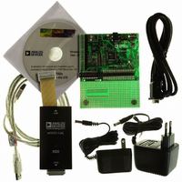
KIT DEV ADUC7026/7027 QUICK PLUS
Manufacturer
Analog Devices Inc
Series
QuickStart™ PLUS Kitr
Type
MCUr
Specifications of EVAL-ADUC7026QSPZ
Contents
Evaluation Board, Power Supply, Cable, Software, Emulator and Documentation
Silicon Manufacturer
Analog Devices
Core Architecture
ARM
Core Sub-architecture
ARM7TDMI
Silicon Core Number
ADuC7026
Rohs Compliant
Yes
Lead Free Status / RoHS Status
Lead free / RoHS Compliant
For Use With/related Products
ADuC7026
Lead Free Status / Rohs Status
Compliant
Available stocks
Company
Part Number
Manufacturer
Quantity
Price
Company:

Part Number:
EVAL-ADUC7026QSPZ
Manufacturer:
Analog Devices Inc
Quantity:
135


EXECUTION TIME FROM SRAM AND FLASH/EE
Execution from SRAM
Fetching instructions from SRAM takes one clock cycle as the
access time of the SRAM is 2 ns and a clock cycle is 22 ns
minimum. However, if the instruction involves reading or
writing data to memory, one extra cycle must be added if the
data is in SRAM (or three cycles if the data is in Flash/EE); one
cycle to execute the instruction, and two cycles to get the 32-bit
data from Flash/EE. A control flow instruction (a branch
instruction, for example) takes one cycle to fetch but also takes
two cycles to fill the pipeline with the new instructions.
Execution from Flash/EE
Because the Flash/EE width is 16 bits and access time for 16-bit
words is 22 ns, execution from Flash/EE cannot be done in
one cycle (as can be done from SRAM when CD Bit = 0). Also,
some dead times are needed before accessing data for any value
of CD bits.
In ARM mode, where instructions are 32 bits, two cycles are
needed to fetch any instruction when CD = 0. In thumb mode,
where instructions are 16 bits, one cycle is needed to fetch any
instruction.
Timing is identical in both modes when executing instructions
that involve using the Flash/EE for data memory. If the
instruction to be executed is a control flow instruction, an extra
cycle is needed to decode the new address of the program
counter, and then four cycles are needed to fill the pipeline. A
data-processing instruction involving only the core register
does not require any extra clock cycles. However, if it involves
data in Flash/EE, an extra clock cycle is needed to decode the
address of the data, and two cycles are needed to get the 32-bit
data from Flash/EE. An extra cycle must also be added before
fetching another instruction. Data transfer instructions are
more complex and are summarized in Table 24.
Table 24. Execution Cycles in ARM/Thumb Mode
Instructions
LD
LDH
LDM/PUSH
STR
STRH
STRM/POP
1
2
The SWAP instruction combines an LD and STR instruction with only one
fetch, giving a total of eight cycles + 40 ns.
N is the number of data to load or store in the multiple load/store instruction
(1 < N ≤ 16).
1
1
Fetch
Cycles
2/1
2/1
2/1
2/1
2/1
2/1
Dead
Time
1
1
N
1
1
N
2
1
Data Access
2
1
2 × N
2 × 20 ns
20 ns
2 × N × 20 ns
2
1
Dead
Time
1
1
N
1
1
N
1
1
Rev. B | Page 47 of 92
RESET AND REMAP
The ARM exception vectors are all situated at the bottom of the
memory array, from Address 0x00000000 to Address 0x00000020
as shown in Figure 51.
By default, and after any reset, the Flash/EE is mirrored at the
bottom of the memory array. The remap function allows the
programmer to mirror the SRAM at the bottom of the memory
array, which facilitates execution of exception routines from
SRAM instead of from Flash/EE. This means exceptions are
executed twice as fast, being executed in 32-bit ARM mode with
32-bit wide SRAM instead of 16-bit wide Flash/EE memory.
Remap Operation
When a reset occurs on the ADuC7019/20/21/22/24/25/26/27/28,
execution automatically starts in factory-programmed, internal
configuration code. This kernel is hidden and cannot be accessed
by user code. If the part is in normal mode (BM pin is high), it
executes the power-on configuration routine of the kernel and
then jumps to the reset vector address, 0x00000000, to execute
the user’s reset exception routine.
Because the Flash/EE is mirrored at the bottom of the memory
array at reset, the reset interrupt routine must always be written
in Flash/EE.
The remap is done from Flash/EE by setting Bit 0 of the REMAP
register. Caution must be taken to execute this command from
Flash/EE, above Address 0x00080020, and not from the bottom
of the array, as this is replaced by the SRAM.
This operation is reversible. The Flash/EE can be remapped at
Address 0x00000000 by clearing Bit 0 of the REMAP MMR.
Caution must again be taken to execute the remap function
from outside the mirrored area. Any type of reset remaps the
Flash/EE memory at the bottom of the array.
KERNEL
INTERRUPT
SERVICE ROUTINES
INTERRUPT
SERVICE ROUTINES
ARM EXCEPTION
VECTOR ADDRESSES
ADuC7019/20/21/22/24/25/26/27/28
Figure 51. Remap for Exception Execution
0x00000020
0x00000000 0x00000000
0x00080000
0x00010000
0xFFFFFFFF
0x0008FFFF
0x00011FFF
FLASH/EE
SRAM
MIRROR SPACE
Related parts for EVAL-ADUC7026QSPZ
Image
Part Number
Description
Manufacturer
Datasheet
Request
R

Part Number:
Description:
IC, ADJ LDO REG, 1.5V TO 5V 250mA MSOP-8
Manufacturer:
Vishay
Datasheet:

Part Number:
Description:
IC, ADJ LDO REG, 1.5V TO 5V 0.6A 8-TSSOP
Manufacturer:
Vishay
Datasheet:
Part Number:
Description:
IC, ADJ LDO REG, 1.5V TO 5V 250mA MSOP-8
Manufacturer:
Vishay
Datasheet:

Part Number:
Description:
IC ADJ LDO REG 1.5V TO 5V 150mA 5-SOT-23
Manufacturer:
Vishay
Datasheet:

Part Number:
Description:
BOARD EVAL AS1324-AD
Manufacturer:
austriamicrosystems
Datasheet:
Part Number:
Description:
IC, ADJ LDO REG, 1.5V TO 5V 0.6A 8-TSSOP
Manufacturer:
Vishay
Datasheet:

Part Number:
Description:
IC, ADJ LDO REG, 1.5V TO 5V, 0.3A, MSOP8
Manufacturer:
Vishay
Datasheet:
Part Number:
Description:
IC, ADJ LDO REG, 1.5V TO 5V, 0.3A, MSOP8
Manufacturer:
Vishay
Datasheet:
Part Number:
Description:
IC, ADJ LDO REG 1.215V TO 5V 0.3A MSOP-8
Manufacturer:
Vishay
Datasheet:
Part Number:
Description:
IC, ADJ LDO REG 1.215V TO 5V 0.3A MSOP-8
Manufacturer:
Vishay
Datasheet:

Part Number:
Description:
±1.7g Dual-Axis IMEMS Accelerometer Evaluation Board
Manufacturer:
Analog Devices Inc
Datasheet:

Part Number:
Description:
IC MULTIPLIER ANALOG 8-SOIC T/R
Manufacturer:
Analog Devices Inc
Datasheet:

Part Number:
Description:
IC ANALOG MULTIPLIER 8-DIP
Manufacturer:
Analog Devices Inc
Datasheet:
Part Number:
Description:
IC ANALOG MULTIPLIER 8-SOIC
Manufacturer:
Analog Devices Inc
Datasheet:
Part Number:
Description:
IC ANALOG MULTIPLIER 8-DIP
Manufacturer:
Analog Devices Inc
Datasheet: