EVAL-ADUC7128QSPZ Analog Devices Inc, EVAL-ADUC7128QSPZ Datasheet - Page 50
EVAL-ADUC7128QSPZ
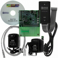
Manufacturer Part Number
EVAL-ADUC7128QSPZ
Description
KIT DEV FOR ADUC7128
Manufacturer
Analog Devices Inc
Series
QuickStart™ PLUS Kitr
Type
MCUr
Datasheet
1.EVAL-ADUC7128QSPZ.pdf
(92 pages)
Specifications of EVAL-ADUC7128QSPZ
Contents
Evaluation Board, Power Supply, Cable, Software, Emulator and Documentation
Silicon Manufacturer
Analog Devices
Core Architecture
ARM
Core Sub-architecture
ARM7TDMI
Silicon Core Number
ADuC7128
Rohs Compliant
Yes
Lead Free Status / RoHS Status
Lead free / RoHS Compliant
For Use With/related Products
ADuC7128
Lead Free Status / RoHS Status
Lead free / RoHS Compliant, Lead free / RoHS Compliant


ADuC7128/ADuC7129
Table 58. Operating Modes
Mode
Active
Pause
Nap
Sleep
Stop
Table 59. Typical Current Consumption at 25°C
PC[2:0]
000
001
010
011
100
MMRs and Keys
To prevent accidental programming, a certain sequence must be
followed when writing in the PLLCON and POWCON registers
(see Table 60).
PLLKEYx Register
Name
PLLKEY1
PLLKEY2
PLLCON Register
Name
PLLCON
POWKEYx Register
Name
POWKEY1
POWKEY2
POWCON Register
Name
POWCON
Table 60. PLLCON and POWCON Write Sequence
PLLCON
PLLKEY1 = 0xAA
PLLCON = 0x01
PLLKEY2 = 0x55
Core
On
Mode
Active
Pause
Nap
Sleep
Stop
Address
0xFFFF0410
0xFFFF0418
Address
0xFFFF0414
Address
0xFFFF0408
Address
0xFFFF0404
0xFFFF040C
Peripherals
On
On
CD = 0
33.1
22.7
3.8
0.4
0.4
Default Value
0x0000
0x0000
Default Value
0x21
Default Value
0x0003
Default Value
0x0000
0x0000
POWCON
POWKEY1 = 0x01
POWCON = user value
POWKEY2 = 0xF4
CD = 1
21.2
13.3
3.8
0.4
0.4
PLL
On
On
On
Access
W
W
Access
R/W
Access
R/W
Access
W
W
XTAL/T2/T3
On
On
On
On
CD = 2
13.8
8.5
3.8
0.4
0.4
Rev. 0 | Page 50 of 92
CD = 3
10
6.1
3.8
0.4
0.4
Table 61. PLLCON MMR Bit Designations
Bit
7:6
5
4:2
1:0
Table 62. POWCON MMR Bit Designations
Bit
7
6:4
3
2:0
Value
000
001
010
011
100
Others
000
001
010
011
100
101
110
111
Value
00
01
10
11
XIRQ
On
On
On
On
On
CD = 4
8.1
4.9
3.8
0.4
0.4
Name
PC
RSVD
CD
Name
OSEL
MDCLK
Start-Up/Power-On Time
130 ms at CD = 0
24 ns at CD = 0; 3.06 μs at CD = 7
24 ns at CD = 0; 3.06 μs at CD = 7
1.58 ms
1.7 ms
CD = 5
7.2
4.3
3.8
0.4
0.4
Description
Reserved.
Operating Modes.
Active mode.
Pause mode.
Nap.
Sleep mode. IRQ0 to IRQ3 and Timer2
can wake up the
ADuC7128/ADuC7129.
Stop mode.
Reserved.
Reserved.
CPU Clock Divider Bits.
41.779200 MHz.
20.889600 MHz.
10.444800 MHz.
5.222400 MHz.
2.611200 MHz.
1.305600 MHz.
654.800 kHz.
326.400 kHz.
Description
Reserved.
32 kHz PLL Input Selection.
Reserved.
Clocking Modes.
Reserved.
PLL. Default configuration.
Reserved.
External clock on P0.7 pin.
Set by user to use the internal
32 kHz oscillator.
Set by default.
Cleared by user to use the
external 32 kHz crystal.
CD = 6
6.7
4
3.8
0.4
0.4
CD = 7
6.45
3.85
3.8
0.4
0.4
Related parts for EVAL-ADUC7128QSPZ
Image
Part Number
Description
Manufacturer
Datasheet
Request
R

Part Number:
Description:
IC, ADJ LDO REG, 1.5V TO 5V 250mA MSOP-8
Manufacturer:
Vishay
Datasheet:

Part Number:
Description:
IC, ADJ LDO REG, 1.5V TO 5V 0.6A 8-TSSOP
Manufacturer:
Vishay
Datasheet:
Part Number:
Description:
IC, ADJ LDO REG, 1.5V TO 5V 250mA MSOP-8
Manufacturer:
Vishay
Datasheet:

Part Number:
Description:
IC ADJ LDO REG 1.5V TO 5V 150mA 5-SOT-23
Manufacturer:
Vishay
Datasheet:

Part Number:
Description:
BOARD EVAL AS1324-AD
Manufacturer:
austriamicrosystems
Datasheet:
Part Number:
Description:
IC, ADJ LDO REG, 1.5V TO 5V 0.6A 8-TSSOP
Manufacturer:
Vishay
Datasheet:

Part Number:
Description:
IC, ADJ LDO REG, 1.5V TO 5V, 0.3A, MSOP8
Manufacturer:
Vishay
Datasheet:
Part Number:
Description:
IC, ADJ LDO REG, 1.5V TO 5V, 0.3A, MSOP8
Manufacturer:
Vishay
Datasheet:
Part Number:
Description:
IC, ADJ LDO REG 1.215V TO 5V 0.3A MSOP-8
Manufacturer:
Vishay
Datasheet:
Part Number:
Description:
IC, ADJ LDO REG 1.215V TO 5V 0.3A MSOP-8
Manufacturer:
Vishay
Datasheet:

Part Number:
Description:
±1.7g Dual-Axis IMEMS Accelerometer Evaluation Board
Manufacturer:
Analog Devices Inc
Datasheet:

Part Number:
Description:
IC MULTIPLIER ANALOG 8-SOIC T/R
Manufacturer:
Analog Devices Inc
Datasheet:

Part Number:
Description:
IC ANALOG MULTIPLIER 8-DIP
Manufacturer:
Analog Devices Inc
Datasheet:
Part Number:
Description:
IC ANALOG MULTIPLIER 8-SOIC
Manufacturer:
Analog Devices Inc
Datasheet:
Part Number:
Description:
IC ANALOG MULTIPLIER 8-DIP
Manufacturer:
Analog Devices Inc
Datasheet: