EVAL-ADUC7128QSPZ Analog Devices Inc, EVAL-ADUC7128QSPZ Datasheet - Page 37
EVAL-ADUC7128QSPZ
Manufacturer Part Number
EVAL-ADUC7128QSPZ
Description
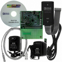
KIT DEV FOR ADUC7128
Manufacturer
Analog Devices Inc
Series
QuickStart™ PLUS Kitr
Type
MCUr
Datasheet
1.EVAL-ADUC7128QSPZ.pdf
(92 pages)
Specifications of EVAL-ADUC7128QSPZ
Contents
Evaluation Board, Power Supply, Cable, Software, Emulator and Documentation
Silicon Manufacturer
Analog Devices
Core Architecture
ARM
Core Sub-architecture
ARM7TDMI
Silicon Core Number
ADuC7128
Rohs Compliant
Yes
Lead Free Status / RoHS Status
Lead free / RoHS Compliant
For Use With/related Products
ADuC7128
Lead Free Status / RoHS Status
Lead free / RoHS Compliant, Lead free / RoHS Compliant


For ac applications, removing high frequency components from
the analog input signal is recommended through the use of an
RC low-pass filter on the relevant analog input pins. In applications
where harmonic distortion and signal-to-noise ratio are critical,
the analog input should be driven from a low impedance source.
Large source impedances significantly affect the ac performance
of the ADC and can necessitate the use of an input buffer amplifier.
The choice of the op amp is a function of the particular application.
Figure 42 and Figure 43 give an example of an ADC front end.
When no amplifier is used to drive the analog input, the source
impedance should be limited to values lower than 1 kΩ. The
maximum source impedance depends on the amount of total
harmonic distortion (THD) that can be tolerated. The THD
increases as the source impedance increases and the
performance degrades.
DRIVING THE ANALOG INPUTS
Internal or external reference can be used for the ADC. In
differential mode of operation, there are restrictions on the
common-mode input signal (V
reference value and supply voltage used to ensure that the signal
remains within the supply rails.
V
CM
minimum and V
Conversion Phase: Switches Open, Track Phase: Switches Closed
Figure 42. Buffering Single-Ended/Pseudo Differential Input
V
REF
Figure 41. Equivalent Analog Input Circuit
Figure 43. Buffering Differential Inputs
C1
C1
CM
AV
AV
maximum values.
DD
DD
10Ω
D
D
D
D
0.01µF
CM
Table 39
) that are dependent on
R1 C2
R1 C2
ADuC7128
ADC0
ADC1
ADuC7128
ADC0
gives some calculated
Rev. 0 | Page 37 of 92
Table 39. V
AV
3.3 V
3.0 V
TEMPERATURE SENSOR
The ADuC7128/ADuC7129 provide a voltage output from an
on-chip band gap reference proportional to absolute temperature.
The voltage output can also be routed through the front end
ADC multiplexer (effectively an additional ADC channel
input), facilitating an internal temperature sensor channel,
measuring die temperature to an accuracy of ±3°C.
The following is a code example of how to configure the ADC
for use with the temperature sensor:
int main(void)
{
float a = 0;
short b;
ADCCON = 0x20;
delay(2000);
ADCCP = 0x10; // Select Temperature Sensor as
REFCON = 0x01;// connect internal 2.5V
ADCCON = 0xE4;// continuous conversion
the formula:
Voltage) / 1.3)
printf("Temperature: %d oC\n",b);
}
DD
a = 0x525 - b;
while(1)
{
while (!ADCSTA){};
b = (ADCDAT >> 16);
// To calculate temperature in °C, use
// ((Temperature = 0x525 - Sensor
a /= 1.3;
b = floor(a);
}
return 0;
V
2.5 V
2.048 V
1.25 V
2.5 V
2.048 V
1.25 V
REF
CM
Ranges
V
1.25 V
1.024 V
0.75 V
1.25 V
1.024 V
0.75 V
// an input to the ADC
// reference to Vref pin
CM
Min
V
2.05 V
2.276 V
2.55 V
1.75 V
1.976 V
2.25 V
ADuC7128/ADuC7129
CM
// power-on the ADC
Max
Signal Peak-to-Peak
2.5 V
2.048 V
1.25 V
2.5 V
2.048 V
1.25 V
Related parts for EVAL-ADUC7128QSPZ
Image
Part Number
Description
Manufacturer
Datasheet
Request
R

Part Number:
Description:
IC, ADJ LDO REG, 1.5V TO 5V 250mA MSOP-8
Manufacturer:
Vishay
Datasheet:

Part Number:
Description:
IC, ADJ LDO REG, 1.5V TO 5V 0.6A 8-TSSOP
Manufacturer:
Vishay
Datasheet:
Part Number:
Description:
IC, ADJ LDO REG, 1.5V TO 5V 250mA MSOP-8
Manufacturer:
Vishay
Datasheet:

Part Number:
Description:
IC ADJ LDO REG 1.5V TO 5V 150mA 5-SOT-23
Manufacturer:
Vishay
Datasheet:

Part Number:
Description:
BOARD EVAL AS1324-AD
Manufacturer:
austriamicrosystems
Datasheet:
Part Number:
Description:
IC, ADJ LDO REG, 1.5V TO 5V 0.6A 8-TSSOP
Manufacturer:
Vishay
Datasheet:

Part Number:
Description:
IC, ADJ LDO REG, 1.5V TO 5V, 0.3A, MSOP8
Manufacturer:
Vishay
Datasheet:
Part Number:
Description:
IC, ADJ LDO REG, 1.5V TO 5V, 0.3A, MSOP8
Manufacturer:
Vishay
Datasheet:
Part Number:
Description:
IC, ADJ LDO REG 1.215V TO 5V 0.3A MSOP-8
Manufacturer:
Vishay
Datasheet:
Part Number:
Description:
IC, ADJ LDO REG 1.215V TO 5V 0.3A MSOP-8
Manufacturer:
Vishay
Datasheet:

Part Number:
Description:
±1.7g Dual-Axis IMEMS Accelerometer Evaluation Board
Manufacturer:
Analog Devices Inc
Datasheet:

Part Number:
Description:
IC MULTIPLIER ANALOG 8-SOIC T/R
Manufacturer:
Analog Devices Inc
Datasheet:

Part Number:
Description:
IC ANALOG MULTIPLIER 8-DIP
Manufacturer:
Analog Devices Inc
Datasheet:
Part Number:
Description:
IC ANALOG MULTIPLIER 8-SOIC
Manufacturer:
Analog Devices Inc
Datasheet:
Part Number:
Description:
IC ANALOG MULTIPLIER 8-DIP
Manufacturer:
Analog Devices Inc
Datasheet: