OM11014 NXP Semiconductors, OM11014 Datasheet - Page 38
OM11014
Manufacturer Part Number
OM11014
Description
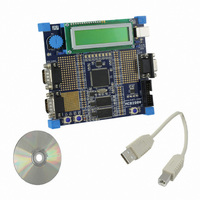
BOARD EVAL FOR LPC2919
Manufacturer
NXP Semiconductors
Series
Keilr
Type
MCUr
Datasheet
1.OM11014.pdf
(67 pages)
Specifications of OM11014
Contents
Board, Cable, CD
For Use With/related Products
LPC2919
Lead Free Status / RoHS Status
Not applicable / Not applicable
Other names
568-4360


NXP Semiconductors
LPC2917_19_1
Product data sheet
8.7.6.4 Master and slave mode
8.7.6.5 PWM pin description
8.7.6.6 PWM clock description
8.7.7.1 Overview
8.7.7 Timers in the MSCSS
A PWM module can provide synchronization signals to other modules (also called Master
mode). The signal sync_out is a pulse of one clock cycle generated when the internal
PWM counter (re)starts. The signal trans_enable_out is a pulse synchronous to sync_out,
generated if a transfer from system registers to PWM shadow registers occurred when the
PWM counter restarted. A delay may be inserted between the counter start and
generation of trans_enable_out and sync_out.
A PWM module can use input signals trans_enable_in and sync_in to synchronize its
internal PWM counter and the transfer of shadow registers (Slave mode).
Each of the four PWM modules in the MSCSS has the following pins. These are combined
with other functions on the port pins of the LPC2917/19.
PWM3 pins.
Table 21.
The PWM modules are clocked by CLK_MSCSS_PWMx (x = 0-3), see
Note that each PWM has its own CLK_MSCSS_PWMx branch clock for power
management. The frequency of all these clocks is identical to CLK_MSCSS_APB since
they are derived from the same base clock BASE_MSCSS_CLK.
Also note that unlike the timer modules in the Peripheral SubSystem, the actual timer
counter registers of the PWM modules run at the same clock as the APB system interface
CLK_MSCSS_APB. This clock is independent of the AHB system clock.
If a PWM module is not used its CLK_MSCSS_PWMx branch clock can be switched off.
The two timers in the MSCSS are functionally identical to the timers in the peripheral
subsystem, see
the timers in the peripheral subsystem, but the capture inputs and match outputs are not
available on the device pins. These signals are instead connected to the ADC and PWM
modules as outlined in the description of the MSCSS, see
Symbol
PWMn CAP[0]
PWMn CAP[1]
PWMn CAP[2]
PWMn MAT[0]
PWMn MAT[1]
PWMn MAT[2]
PWMn MAT[3]
PWMn MAT[4]
PWMn MAT[5]
PWMn TRAP
PWM pins
Section
Direction
IN
IN
IN
OUT
OUT
OUT
OUT
OUT
OUT
IN
Rev. 01 — 31 July 2008
8.4.3. The features of the timers in the MSCSS are the same as
Description
PWM n capture input 0
PWM n capture input 1
PWM n capture input 2
PWM n match output 0
PWM n match output 1
PWM n match output 2
PWM n match output 3
PWM n match output 4
PWM n match output 5
PWM n trap input
ARM9 microcontroller with CAN and LIN
Table 21
Section
LPC2917/19
shows the PWM0 to
8.7.2.
© NXP B.V. 2008. All rights reserved.
Section
7.2.2.
38 of 67
Related parts for OM11014
Image
Part Number
Description
Manufacturer
Datasheet
Request
R

Part Number:
Description:
NXP Semiconductors designed the LPC2420/2460 microcontroller around a 16-bit/32-bitARM7TDMI-S CPU core with real-time debug interfaces that include both JTAG andembedded trace
Manufacturer:
NXP Semiconductors
Datasheet:

Part Number:
Description:
NXP Semiconductors designed the LPC2458 microcontroller around a 16-bit/32-bitARM7TDMI-S CPU core with real-time debug interfaces that include both JTAG andembedded trace
Manufacturer:
NXP Semiconductors
Datasheet:
Part Number:
Description:
NXP Semiconductors designed the LPC2468 microcontroller around a 16-bit/32-bitARM7TDMI-S CPU core with real-time debug interfaces that include both JTAG andembedded trace
Manufacturer:
NXP Semiconductors
Datasheet:
Part Number:
Description:
NXP Semiconductors designed the LPC2470 microcontroller, powered by theARM7TDMI-S core, to be a highly integrated microcontroller for a wide range ofapplications that require advanced communications and high quality graphic displays
Manufacturer:
NXP Semiconductors
Datasheet:
Part Number:
Description:
NXP Semiconductors designed the LPC2478 microcontroller, powered by theARM7TDMI-S core, to be a highly integrated microcontroller for a wide range ofapplications that require advanced communications and high quality graphic displays
Manufacturer:
NXP Semiconductors
Datasheet:
Part Number:
Description:
The Philips Semiconductors XA (eXtended Architecture) family of 16-bit single-chip microcontrollers is powerful enough to easily handle the requirements of high performance embedded applications, yet inexpensive enough to compete in the market for hi
Manufacturer:
NXP Semiconductors
Datasheet:
Part Number:
Description:
The XA-S3 device is a member of Philips Semiconductors? XA(eXtended Architecture) family of high performance 16-bitsingle-chip microcontrollers
Manufacturer:
NXP Semiconductors
Datasheet:

Part Number:
Description:
The NXP BlueStreak LH75401/LH75411 family consists of two low-cost 16/32-bit System-on-Chip (SoC) devices
Manufacturer:
NXP Semiconductors
Datasheet:
Part Number:
Description:
The NXP LPC3130/3131 combine an 180 MHz ARM926EJ-S CPU core, high-speed USB2
Manufacturer:
NXP Semiconductors
Datasheet:
Part Number:
Description:
The NXP LPC3141 combine a 270 MHz ARM926EJ-S CPU core, High-speed USB 2
Manufacturer:
NXP Semiconductors
Part Number:
Description:
The NXP LPC3143 combine a 270 MHz ARM926EJ-S CPU core, High-speed USB 2
Manufacturer:
NXP Semiconductors

Part Number:
Description:
The NXP LPC3152 combines an 180 MHz ARM926EJ-S CPU core, High-speed USB 2
Manufacturer:
NXP Semiconductors
Part Number:
Description:
The NXP LPC3154 combines an 180 MHz ARM926EJ-S CPU core, High-speed USB 2
Manufacturer:
NXP Semiconductors

Part Number:
Description:
Standard level N-channel enhancement mode Field-Effect Transistor (FET) in a plastic package using NXP High-Performance Automotive (HPA) TrenchMOS technology
Manufacturer:
NXP Semiconductors
Datasheet: