OM11014 NXP Semiconductors, OM11014 Datasheet - Page 26
OM11014
Manufacturer Part Number
OM11014
Description
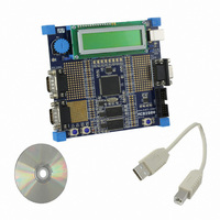
BOARD EVAL FOR LPC2919
Manufacturer
NXP Semiconductors
Series
Keilr
Type
MCUr
Datasheet
1.OM11014.pdf
(67 pages)
Specifications of OM11014
Contents
Board, Cable, CD
For Use With/related Products
LPC2919
Lead Free Status / RoHS Status
Not applicable / Not applicable
Other names
568-4360


NXP Semiconductors
LPC2917_19_1
Product data sheet
8.4.4.4 UART clock description
8.4.5.1 Overview
8.4.5.2 Functional description
8.4.5 Serial peripheral interface
The UART modules are clocked by two different clocks; CLK_SYS_PESS and
CLK_UARTx (x = 0-1), see
branch clock for power management. The frequency of all CLK_UARTx clocks is identical
since they are derived from the same base clock BASE_CLK_UART. The register
interface towards the system bus is clocked by CLK_SYS_PESS. The baud generator is
clocked by the CLK_UARTx.
The LPC2917/19 contains three SPI modules to allow synchronous serial communication
with slave or master peripherals.
The key features are:
The SPI module is a master or slave interface for synchronous serial communication with
peripheral devices that have either Motorola SPI or Texas Instruments Synchronous Serial
Interfaces.
The SPI module performs serial-to-parallel conversion on data received from a peripheral
device. The transmit and receive paths are buffered with FIFO memories (16 bits wide
32 words deep). Serial data is transmitted on SPI_TXD and received on SPI_RXD.
The SPI module includes a programmable bit-rate clock divider and prescaler to generate
the SPI serial clock from the input clock CLK_SPIx.
The SPI module’s operating mode, frame format, and word size are programmed through
the SLVn_SETTINGS registers.
A single combined interrupt request SPI_INTREQ output is asserted if any of the
interrupts are asserted and unmasked.
•
•
•
•
•
•
•
•
•
•
•
Master or slave operation
Supports up to four slaves in sequential multi-slave operation
Supports timer-triggered operation
Programmable clock bit rate and prescale based on SPI source clock
(BASE_SPI_CLK), independent of system clock
Separate transmit and receive FIFO memory buffers; 16 bits wide, 32 locations deep
Programmable choice of interface operation: Motorola SPI or Texas Instruments
Synchronous Serial Interfaces
Programmable data-frame size from 4 to 16 bits
Independent masking of transmit FIFO, receive FIFO and receive overrun interrupts
Serial clock-rate master mode: fserial_clk
Serial clock-rate slave mode: fserial_clk = f
Internal loopback test mode
Rev. 01 — 31 July 2008
Section
7.2.2. Note that each UART has its own CLK_UARTx
ARM9 microcontroller with CAN and LIN
CLK(SPI)*
f
CLK(SPI)*
/4
/2
LPC2917/19
© NXP B.V. 2008. All rights reserved.
26 of 67
Related parts for OM11014
Image
Part Number
Description
Manufacturer
Datasheet
Request
R

Part Number:
Description:
NXP Semiconductors designed the LPC2420/2460 microcontroller around a 16-bit/32-bitARM7TDMI-S CPU core with real-time debug interfaces that include both JTAG andembedded trace
Manufacturer:
NXP Semiconductors
Datasheet:

Part Number:
Description:
NXP Semiconductors designed the LPC2458 microcontroller around a 16-bit/32-bitARM7TDMI-S CPU core with real-time debug interfaces that include both JTAG andembedded trace
Manufacturer:
NXP Semiconductors
Datasheet:
Part Number:
Description:
NXP Semiconductors designed the LPC2468 microcontroller around a 16-bit/32-bitARM7TDMI-S CPU core with real-time debug interfaces that include both JTAG andembedded trace
Manufacturer:
NXP Semiconductors
Datasheet:
Part Number:
Description:
NXP Semiconductors designed the LPC2470 microcontroller, powered by theARM7TDMI-S core, to be a highly integrated microcontroller for a wide range ofapplications that require advanced communications and high quality graphic displays
Manufacturer:
NXP Semiconductors
Datasheet:
Part Number:
Description:
NXP Semiconductors designed the LPC2478 microcontroller, powered by theARM7TDMI-S core, to be a highly integrated microcontroller for a wide range ofapplications that require advanced communications and high quality graphic displays
Manufacturer:
NXP Semiconductors
Datasheet:
Part Number:
Description:
The Philips Semiconductors XA (eXtended Architecture) family of 16-bit single-chip microcontrollers is powerful enough to easily handle the requirements of high performance embedded applications, yet inexpensive enough to compete in the market for hi
Manufacturer:
NXP Semiconductors
Datasheet:
Part Number:
Description:
The XA-S3 device is a member of Philips Semiconductors? XA(eXtended Architecture) family of high performance 16-bitsingle-chip microcontrollers
Manufacturer:
NXP Semiconductors
Datasheet:

Part Number:
Description:
The NXP BlueStreak LH75401/LH75411 family consists of two low-cost 16/32-bit System-on-Chip (SoC) devices
Manufacturer:
NXP Semiconductors
Datasheet:
Part Number:
Description:
The NXP LPC3130/3131 combine an 180 MHz ARM926EJ-S CPU core, high-speed USB2
Manufacturer:
NXP Semiconductors
Datasheet:
Part Number:
Description:
The NXP LPC3141 combine a 270 MHz ARM926EJ-S CPU core, High-speed USB 2
Manufacturer:
NXP Semiconductors
Part Number:
Description:
The NXP LPC3143 combine a 270 MHz ARM926EJ-S CPU core, High-speed USB 2
Manufacturer:
NXP Semiconductors

Part Number:
Description:
The NXP LPC3152 combines an 180 MHz ARM926EJ-S CPU core, High-speed USB 2
Manufacturer:
NXP Semiconductors
Part Number:
Description:
The NXP LPC3154 combines an 180 MHz ARM926EJ-S CPU core, High-speed USB 2
Manufacturer:
NXP Semiconductors

Part Number:
Description:
Standard level N-channel enhancement mode Field-Effect Transistor (FET) in a plastic package using NXP High-Performance Automotive (HPA) TrenchMOS technology
Manufacturer:
NXP Semiconductors
Datasheet: