OM11014 NXP Semiconductors, OM11014 Datasheet - Page 10
OM11014
Manufacturer Part Number
OM11014
Description
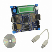
BOARD EVAL FOR LPC2919
Manufacturer
NXP Semiconductors
Series
Keilr
Type
MCUr
Datasheet
1.OM11014.pdf
(67 pages)
Specifications of OM11014
Contents
Board, Cable, CD
For Use With/related Products
LPC2919
Lead Free Status / RoHS Status
Not applicable / Not applicable
Other names
568-4360


NXP Semiconductors
Table 3.
7. Functional description
1.
LPC2917_19_1
Product data sheet
Pin name
P2[17]/RXD1/PCAP1[0]/BLS3
V
P0[18]/IN2[2]/PMAT2[0]/A14
P0[19]/IN2[3]/PMAT2[1]/A15
P3[4]/MAT3[2]/PMAT2[4]/TXDC1
P3[5]/MAT3[3]/PMAT2[5]/RXDC1
P2[18]/PCAP1[1]/D16
P2[19]/PCAP1[2]/D17
P0[20]/IN2[4]/PMAT2[2]/A16
P0[21]/IN2[5]/PMAT2[3]/A17
P0[22]/IN2[6]/PMAT2[4]/A18
V
P0[23]/IN2[7]/PMAT2[5]/A19
P2[20]/PCAP2[0]/D18
TDI
DD(IO)
SS(IO)
Only for 1.8 V power sources
LQFP144 pin assignment
7.1.1 Reset and power-up behavior
7.1.2 Reset strategy
7.1 Reset, debug, test and power description
The LPC2917/19 contains external reset input and internal power-up reset circuits. This
ensures that a reset is extended internally until the oscillators and flash have reached a
stable state. See
Section 12
the reset pin.
Table 4.
At activation of the RST_N pin the JTAGSEL pin is sensed as logic LOW. If this is the case
the LPC2917/19 is assumed to be connected to debug hardware, and internal circuits
reprogram the source for the BASE_SYS_CLK to be the crystal oscillator instead of the
Low-Power Ring Oscillator (LP_OSC). This is required because the clock rate when
running at LP_OSC speed is too low for the external debugging environment.
The LPC2917/19 contains a central module, the Reset Generation Unit (RGU) in the
Power, Clock and Reset SubSystem (PCRSS), which controls all internal reset signals
towards the peripheral modules. The RGU provides individual reset control as well as the
monitoring functions needed for tracing a reset back to source.
Symbol
RST_N
Reset pin
for characteristics of the several start-up and initialization times.
Pin
130
131
132
133
134
135
136
137
138
139
140
141
142
143
144
…continued
Direction
IN
Description
Default function
GPIO 2, pin 17
3.3 V power supply for I/O
GPIO 0, pin 18
GPIO 0, pin 19
GPIO 3, pin 4
GPIO 3, pin 5
GPIO 2, pin 18
GPIO 2, pin 19
GPIO 0, pin 20
GPIO 0, pin 21
GPIO 0, pin 22
ground for I/O
GPIO 0, pin 23
GPIO 2, pin 20
IEEE 1149.1 data in, pulled up internally
Section 11
Rev. 01 — 31 July 2008
Description
external reset input, active LOW; pulled up internally
for trip levels of the internal power-up reset circuit
Function 1
UART1 RXD
ADC2 IN2
ADC2 IN3
TIMER3 MAT2
TIMER3 MAT3
-
-
ADC2 IN4
ADC2 IN5
ADC2 IN6
ADC2 IN7
-
ARM9 microcontroller with CAN and LIN
Function 2
PWM1 CAP0
PWM2 MAT0
PWM2 MAT1
PWM2 MAT4
PWM2 MAT5
PWM1 CAP1
PWM1 CAP2
PWM2 MAT2
PWM2 MAT3
PWM2 MAT4
PWM2 MAT5
PWM2 CAP0
LPC2917/19
© NXP B.V. 2008. All rights reserved.
Function 3
EXTBUS BLS3
EXTBUS A14
EXTBUS A15
CAN1 TXDC
CAN1 RXDC
EXTBUS D16
EXTBUS D17
EXTBUS A16
EXTBUS A17
EXTBUS A18
EXTBUS A19
EXTBUS D18
Table 4
1
. See
shows
10 of 67
Related parts for OM11014
Image
Part Number
Description
Manufacturer
Datasheet
Request
R

Part Number:
Description:
NXP Semiconductors designed the LPC2420/2460 microcontroller around a 16-bit/32-bitARM7TDMI-S CPU core with real-time debug interfaces that include both JTAG andembedded trace
Manufacturer:
NXP Semiconductors
Datasheet:

Part Number:
Description:
NXP Semiconductors designed the LPC2458 microcontroller around a 16-bit/32-bitARM7TDMI-S CPU core with real-time debug interfaces that include both JTAG andembedded trace
Manufacturer:
NXP Semiconductors
Datasheet:
Part Number:
Description:
NXP Semiconductors designed the LPC2468 microcontroller around a 16-bit/32-bitARM7TDMI-S CPU core with real-time debug interfaces that include both JTAG andembedded trace
Manufacturer:
NXP Semiconductors
Datasheet:
Part Number:
Description:
NXP Semiconductors designed the LPC2470 microcontroller, powered by theARM7TDMI-S core, to be a highly integrated microcontroller for a wide range ofapplications that require advanced communications and high quality graphic displays
Manufacturer:
NXP Semiconductors
Datasheet:
Part Number:
Description:
NXP Semiconductors designed the LPC2478 microcontroller, powered by theARM7TDMI-S core, to be a highly integrated microcontroller for a wide range ofapplications that require advanced communications and high quality graphic displays
Manufacturer:
NXP Semiconductors
Datasheet:
Part Number:
Description:
The Philips Semiconductors XA (eXtended Architecture) family of 16-bit single-chip microcontrollers is powerful enough to easily handle the requirements of high performance embedded applications, yet inexpensive enough to compete in the market for hi
Manufacturer:
NXP Semiconductors
Datasheet:
Part Number:
Description:
The XA-S3 device is a member of Philips Semiconductors? XA(eXtended Architecture) family of high performance 16-bitsingle-chip microcontrollers
Manufacturer:
NXP Semiconductors
Datasheet:

Part Number:
Description:
The NXP BlueStreak LH75401/LH75411 family consists of two low-cost 16/32-bit System-on-Chip (SoC) devices
Manufacturer:
NXP Semiconductors
Datasheet:
Part Number:
Description:
The NXP LPC3130/3131 combine an 180 MHz ARM926EJ-S CPU core, high-speed USB2
Manufacturer:
NXP Semiconductors
Datasheet:
Part Number:
Description:
The NXP LPC3141 combine a 270 MHz ARM926EJ-S CPU core, High-speed USB 2
Manufacturer:
NXP Semiconductors
Part Number:
Description:
The NXP LPC3143 combine a 270 MHz ARM926EJ-S CPU core, High-speed USB 2
Manufacturer:
NXP Semiconductors

Part Number:
Description:
The NXP LPC3152 combines an 180 MHz ARM926EJ-S CPU core, High-speed USB 2
Manufacturer:
NXP Semiconductors
Part Number:
Description:
The NXP LPC3154 combines an 180 MHz ARM926EJ-S CPU core, High-speed USB 2
Manufacturer:
NXP Semiconductors

Part Number:
Description:
Standard level N-channel enhancement mode Field-Effect Transistor (FET) in a plastic package using NXP High-Performance Automotive (HPA) TrenchMOS technology
Manufacturer:
NXP Semiconductors
Datasheet: