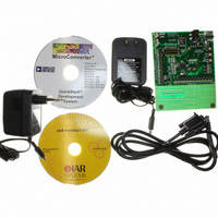
EVAL-ADUC847QSZ Analog Devices Inc, EVAL-ADUC847QSZ Datasheet - Page 59

EVAL-ADUC847QSZ
Manufacturer Part Number
EVAL-ADUC847QSZ
Description
KIT DEV QUICK START FOR ADUC847
Manufacturer
Analog Devices Inc
Series
QuickStart™ Kitr
Type
MCUr
Datasheet
1.EVAL-ADUC845QSZ.pdf
(108 pages)
Specifications of EVAL-ADUC847QSZ
Contents
Evaluation Board, Power Supply, Cable, Software and Documentation
Silicon Manufacturer
Analog Devices
Core Architecture
8051
Silicon Core Number
ADuC847
Tool / Board Applications
General Purpose MCU, MPU, DSP, DSC
Mcu Supported Families
ADUC8xx
Development Tool Type
Hardware - Eval/Demo Board
Rohs Compliant
Yes
Lead Free Status / RoHS Status
Lead free / RoHS Compliant
For Use With/related Products
ADuC847
Lead Free Status / RoHS Status
Lead free / RoHS Compliant, Lead free / RoHS Compliant
Mode 5 (Dual 8-Bit PWM)
In Mode 5, the duty cycle and the resolution of the PWM outputs
are individually programmable. The maximum resolution of the
PWM output is 8 bits.
Mode 6 (Dual RZ 16-Bit Σ-∆ DAC)
Mode 6 provides a high speed PWM output similar to that of a
Σ-Δ DAC. Mode 6 operates very similarly to Mode 4; however,
the key difference is that Mode 6 provides return to zero (RZ)
Σ-Δ DAC output. Mode 4 provides non-return-to-zero Σ-Δ
DAC outputs. RZ mode ensures that any difference in the rise
and fall times does not affect the Σ-Δ DAC INL. However, RZ
mode halves the dynamic range of the Σ-Δ DAC outputs from
0 V− to AV
mode should be used with a PWM clock divider of 4.
If PWM1H is set to 4010H (slightly above one-quarter of FS),
typically P2.6 is low for three full clocks (3 × 80 ns), high for
one-half a clock (40 ns), and then low again for one-half a clock
(40 ns) before repeating itself. Over every 65536 clocks, the
PWM compromises for the fact that the output should be
slightly above one-quarter of full scale by leaving the output
high for two half clocks in four every so often.
For faster DAC outputs (at lower resolution), write 0s to the
LSBs that are not required with a 1 in the LSB position. If, for
example, only 12-bit performance is required, write 0001 to the
4 LSBs. This means that a 12-bit accurate Σ-Δ DAC output can
occur at 3 kHz. Similarly, writing 00000001 to the 8 LSBs gives
an 8-bit accurate Σ-Δ DAC output at 49 kHz.
DD
down to 0 V to AV
PWM COUNTERS
Figure 43. PWM Mode 5
DD
/2. For best results, this
0
P2.5
PWM1H
PWM0H
P2.6
PWM1L
PWM0L
Rev. B | Page 59 of 108
The output resolution is set by the PWM1L and PWM1H SFRs
for the P2.5 and P2.6 outputs, respectively. PWM0L and PWM0H
set the duty cycles of the PWM outputs at P2.5 and P2.6,
respectively. Both PWMs have the same clock source and clock
divider.
Mode 7
In Mode 7, the PWM is disabled, allowing P2.5 and P2.6 to be
used as normal.
PWM1H/L = 4000H
PWM0H/L = C000H
3.146MHz
16-BIT
16-BIT
0, 3/4, 1/2, 1/4, 0
16-BIT
16-BIT
LATCH
ADuC845/ADuC847/ADuC848
Figure 44. PWM Mode 6
CARRY OUT AT P2.5
CARRY OUT AT P2.6
16-BIT
16-BIT
318µs
318µs
0 1
0
0
1
0
1
1
0
0
1
0
1
0


