EVAL-ADUC847QSZ Analog Devices Inc, EVAL-ADUC847QSZ Datasheet - Page 55
EVAL-ADUC847QSZ
Manufacturer Part Number
EVAL-ADUC847QSZ
Description
KIT DEV QUICK START FOR ADUC847
Manufacturer
Analog Devices Inc
Series
QuickStart™ Kitr
Type
MCUr
Datasheet
1.EVAL-ADUC845QSZ.pdf
(108 pages)
Specifications of EVAL-ADUC847QSZ
Contents
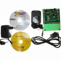
Evaluation Board, Power Supply, Cable, Software and Documentation
Silicon Manufacturer
Analog Devices
Core Architecture
8051
Silicon Core Number
ADuC847
Tool / Board Applications
General Purpose MCU, MPU, DSP, DSC
Mcu Supported Families
ADUC8xx
Development Tool Type
Hardware - Eval/Demo Board
Rohs Compliant
Yes
Lead Free Status / RoHS Status
Lead free / RoHS Compliant
For Use With/related Products
ADuC847
Lead Free Status / RoHS Status
Lead free / RoHS Compliant, Lead free / RoHS Compliant


For larger loads, the current drive capability may not be suffi-
cient. To increase the source and sink current capability of the
DAC, an external buffer should be added as shown in Figure 37.
The internal DAC output buffer also features a high impedance
disable function. In the chip’s default power-on state, the DAC
is disabled and its output is in a high impedance state (or three-
state) where it remains inactive until enabled in software. This
means that if a zero output is desired during power-on or
power-down transient conditions, a pull-down resistor must be
added to each DAC output. Assuming that this resistor is in
place, the DAC output remains at ground potential whenever
the DAC is disabled.
Figure 36. Source and Sink Current Capability with V
3
2
1
0
0
ADuC845/
ADuC847/
ADuC848
DAC LOADED WITH 0FFFH
DAC LOADED WITH 0000H
Figure 37. Buffering the DAC Output
DAC
SOURCE/SINK CURRENT (mA)
5
14
10
REF
= AV
DD
15
= 3 V
Rev. B | Page 55 of 108
PULSE-WIDTH MODULATOR (PWM)
The ADuC845/ADuC847/ADuC848 has a highly flexible PWM
offering programmable resolution and an input clock. The
PWM can be configured in six different modes of operation.
Two of these modes allow the PWM to be configured as a Σ-∆
DAC with up to 16 bits of resolution. A block diagram of the
PWM is shown in Figure 38.
The PWM uses control SFR, PWMCON, and four data SFRs:
PWM0H, PWM0L, PWM1H, and PWM1L.
PWMCON (as described in Table 34) controls the different
modes of operation of the PWM as well as the PWM clock
frequency. PWM0H/L and PWM1H/L are the data registers that
determine the duty cycles of the PWM outputs at P2.5 and P2.6.
To use the PWM user software, first write to PWMCON to
select the PWM mode of operation and the PWM input clock.
Writing to PWMCON also resets the PWM counter. In any of
the 16-bit modes of operation (Modes 1, 3, 4, 6), user software
should write to the PWM0L or PWM1L SFRs first. This value is
written to a hidden SFR. Writing to the PWM0H or PWM1H
SFRs updates both the PWMxH and the PWMxL SFRs but does
not change the outputs until the end of the PWM cycle in
progress. The values written to these 16-bit registers are then
used in the next PWM cycle.
EXTERNAL CLOCK ON P2.7
12.583MHz (F
32.768kHz (F
32.768kHz/15
XTAL)
VCO)
Figure 38. PWM Block Diagram
ADuC845/ADuC847/ADuC848
SELECT
CLOCK
MODE
16-BIT PWM COUNTER
PROGRAMMABLE
COMPARE
PWM0H/L
DIVIDER
PWM1H/L
P2.5
P2.6
Related parts for EVAL-ADUC847QSZ
Image
Part Number
Description
Manufacturer
Datasheet
Request
R


Part Number:
Description:
BOARD EVAL FOR SI270X-A
Manufacturer:
Silicon Laboratories Inc
Datasheet:

Part Number:
Description:
BUCK CONV REF DESIGN KIT IP1201
Manufacturer:
International Rectifier
Datasheet:
Part Number:
Description:
BOARD DEMO SYNC DUAL BUCK CNVTER
Manufacturer:
International Rectifier
Datasheet:
Part Number:
Description:
BOARD DEMO SYNC BUCK CONVETER
Manufacturer:
International Rectifier
Datasheet:

Part Number:
Description:
EVALBOARD/EB Omnidirectional microphone - Analog
Manufacturer:
Analog Devices
Datasheet:
Part Number:
Description:
EVALBOARD/EB Omnidirectional microphone - Analog
Manufacturer:
Analog Devices
Datasheet:


Part Number:
Description:
BOARD EVAL LED DRIVER LT3756
Manufacturer:
Linear Technology
Datasheet:

Part Number:
Description:
BOARD EVAL FOR AD7741/7742
Manufacturer:
Analog Devices Inc
Datasheet:

Part Number:
Description:
±1.7g Dual-Axis IMEMS Accelerometer Evaluation Board
Manufacturer:
Analog Devices Inc
Datasheet:

Part Number:
Description:
IC MULTIPLIER ANALOG 8-SOIC T/R
Manufacturer:
Analog Devices Inc
Datasheet:

Part Number:
Description:
IC ANALOG MULTIPLIER 8-DIP
Manufacturer:
Analog Devices Inc
Datasheet:
Part Number:
Description:
IC ANALOG MULTIPLIER 8-SOIC
Manufacturer:
Analog Devices Inc
Datasheet:
Part Number:
Description:
IC ANALOG MULTIPLIER 8-DIP
Manufacturer:
Analog Devices Inc
Datasheet: