EVAL-ADUC847QSZ Analog Devices Inc, EVAL-ADUC847QSZ Datasheet - Page 26
EVAL-ADUC847QSZ
Manufacturer Part Number
EVAL-ADUC847QSZ
Description
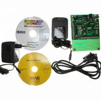
KIT DEV QUICK START FOR ADUC847
Manufacturer
Analog Devices Inc
Series
QuickStart™ Kitr
Type
MCUr
Datasheet
1.EVAL-ADUC845QSZ.pdf
(108 pages)
Specifications of EVAL-ADUC847QSZ
Contents
Evaluation Board, Power Supply, Cable, Software and Documentation
Silicon Manufacturer
Analog Devices
Core Architecture
8051
Silicon Core Number
ADuC847
Tool / Board Applications
General Purpose MCU, MPU, DSP, DSC
Mcu Supported Families
ADUC8xx
Development Tool Type
Hardware - Eval/Demo Board
Rohs Compliant
Yes
Lead Free Status / RoHS Status
Lead free / RoHS Compliant
For Use With/related Products
ADuC847
Lead Free Status / RoHS Status
Lead free / RoHS Compliant, Lead free / RoHS Compliant


ADuC845/ADuC847/ADuC848
ADC CIRCUIT INFORMATION
The ADuC845 incorporates two 10-channel (8-channel on th
MQFP package) 24-bit Σ-∆ ADCs, while the ADuC847 and
ADuC848 each incorporate a single 10-channel (8-channel on
the MQFP package) 24-bit and 16-bit Σ-∆ ADC.
Each part also includes an on-chip programmable gain
amplifier and configurable buffering (neither is ava
auxiliary ADC on the ADuC845). The parts also incorporate
digital filtering intended for measuring wide dynamic range an
low frequency signals such as those in weigh-scale, strain-gage,
pressure transducer, or temperature measurement applicatio
The ADuC845/ADuC847/ADuC848 can be configured as four
or five (MQFP/LFCSP package) fully-differential input channel
or as eight or ten (MQFP/LFCSP package) pseudo differential
input channels referenced to AINCOM. The ADC on each part
(primary only on the ADuC845) can be fully buffered interna
and can be programmed for one of eight inp
±20 mV to ±2.56 V (V
means that the part can handle significant source impedanc
on the selected analog input and that RC filtering (for noise
rejection or RFI reduction) can be placed on the analog inputs
If the ADC is used with internal buffering disabled
(ADC0CON1.7 = 1, ADC0CON1.6 = 0), these unbuffered
inputs provide a dynamic load to the driving source. Therefo
resistor/capacitor combinations on the inputs can cause dc gain
errors, depending on the output impedance of the source that is
driving the ADC in
Table 8 and Table 9 show the allowable external resistance/
capacitance values for unbuffered mode such that no gain error
at the 16-bit and 20-bit levels, respectiv
used with internal buffering enabled, it is recommended that a
Table 8. Maximum Resistance for No 16-Bit Gain Error (Unbuffered Mode)
Gain
1
2
4
8–128
Table 9. Maximum Resistance for No 20-Bit Gain Error (Unbuffered Mode)
Gain
1
2
4
8–128
0 pF
111.3 kΩ
53.7 kΩ
25.4 kΩ
10.7 kΩ
0 pF
84.9 kΩ
42.0 kΩ
20.5 kΩ
8.8 kΩ
puts.
REF
× 1.024). Buffering the input channel
50 pF
21.1 kΩ
10.4 kΩ
5.0 kΩ
2.3 k Ω
50 pF
27.8 kΩ
13.5 kΩ
6.4 kΩ
2.9 kΩ
ely, is introduced. When
ut ranges from
ilable on the
100 pF
12.5 kΩ
6.1 kΩ
2.9 kΩ
1.3 k Ω
100 pF
16.7 kΩ
8.1 kΩ
3.9 kΩ
1.7 kΩ
es
Rev. B | Page 26 of 108
lly,
ns.
re,
e
.
d
s
External Capacitance
External Capacitance
capacitor (10 nF to 100 nF) be placed on the input to the ADC
(usually as part of an antialiasing filter) to aid in noise
performance.
The input channels are intended to convert signals directly from
sensors without the need for external signal conditioning. With
internal buffering disabled (relevant bits set/cleared in
ADC0CON1), external buffering might be required.
When the internal buffer is enabled, it might be necessa
offset the negative input channel by +100 mV and to offset the
positive channel by −100 mV
This accounts for the restricted common-mode input range in
the buffer. Some circuits, for example, bridge circuits, are
inheren
output voltage is balanced around
large to encroach on the supply rails. Internal buffering is no
available
ADC (ADuC845 only) is fixed at a gain range of ±2
The ADCs use a Σ-Δ conversion technique to realize up t
24 bits on the ADuC845 and the ADuC847, and up to 16 bits on
the ADuC848 of no mis
rate, chop enabled). The Σ-Δ modulator converts the sampled
input signal into a digital pulse train whose duty cycle cont
the digital information. A sinc
(see Table 28) is then used to decimate the modulator output
data stream to give a valid da
m
chop enabled and chop disabled. The CHOP
A
DCMODE register enables or disables the chopping scheme.
able output rates. The signal chain has two modes of operation,
500 pF
3.2 kΩ
1.6 kΩ
790 Ω
370 Ω
500 pF
4.5 kΩ
2.2 kΩ
1.0 kΩ
480 Ω
tly suitable to use without having to offset where the
on the auxiliary ADC (ADuC845 only). The auxiliary
1000 pF
1.77 kΩ
880 Ω
430 Ω
195 Ω
1000 pF
2.58 kΩ
1.26 kΩ
600 Ω
270 Ω
sin
g codes performance (20 Hz update
ta conversion result at program-
if the reference range is AV
3
programmable low-pass filter
V
REF
/2 and is not sufficiently
bit in the
5000 pF
440 Ω
220 Ω
110 Ω
50 Ω
5000 pF
360 Ω
75 Ω
700 Ω
170 Ω
.50 V.
ry to
DD
o
ains
.
t
Related parts for EVAL-ADUC847QSZ
Image
Part Number
Description
Manufacturer
Datasheet
Request
R


Part Number:
Description:
BOARD EVAL FOR SI270X-A
Manufacturer:
Silicon Laboratories Inc
Datasheet:

Part Number:
Description:
BUCK CONV REF DESIGN KIT IP1201
Manufacturer:
International Rectifier
Datasheet:
Part Number:
Description:
BOARD DEMO SYNC DUAL BUCK CNVTER
Manufacturer:
International Rectifier
Datasheet:
Part Number:
Description:
BOARD DEMO SYNC BUCK CONVETER
Manufacturer:
International Rectifier
Datasheet:

Part Number:
Description:
EVALBOARD/EB Omnidirectional microphone - Analog
Manufacturer:
Analog Devices
Datasheet:
Part Number:
Description:
EVALBOARD/EB Omnidirectional microphone - Analog
Manufacturer:
Analog Devices
Datasheet:


Part Number:
Description:
BOARD EVAL LED DRIVER LT3756
Manufacturer:
Linear Technology
Datasheet:

Part Number:
Description:
BOARD EVAL FOR AD7741/7742
Manufacturer:
Analog Devices Inc
Datasheet:

Part Number:
Description:
±1.7g Dual-Axis IMEMS Accelerometer Evaluation Board
Manufacturer:
Analog Devices Inc
Datasheet:

Part Number:
Description:
IC MULTIPLIER ANALOG 8-SOIC T/R
Manufacturer:
Analog Devices Inc
Datasheet:

Part Number:
Description:
IC ANALOG MULTIPLIER 8-DIP
Manufacturer:
Analog Devices Inc
Datasheet:
Part Number:
Description:
IC ANALOG MULTIPLIER 8-SOIC
Manufacturer:
Analog Devices Inc
Datasheet:
Part Number:
Description:
IC ANALOG MULTIPLIER 8-DIP
Manufacturer:
Analog Devices Inc
Datasheet: