EVAL-ADUC847QSZ Analog Devices Inc, EVAL-ADUC847QSZ Datasheet - Page 29
EVAL-ADUC847QSZ
Manufacturer Part Number
EVAL-ADUC847QSZ
Description
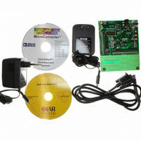
KIT DEV QUICK START FOR ADUC847
Manufacturer
Analog Devices Inc
Series
QuickStart™ Kitr
Type
MCUr
Datasheet
1.EVAL-ADUC845QSZ.pdf
(108 pages)
Specifications of EVAL-ADUC847QSZ
Contents
Evaluation Board, Power Supply, Cable, Software and Documentation
Silicon Manufacturer
Analog Devices
Core Architecture
8051
Silicon Core Number
ADuC847
Tool / Board Applications
General Purpose MCU, MPU, DSP, DSC
Mcu Supported Families
ADUC8xx
Development Tool Type
Hardware - Eval/Demo Board
Rohs Compliant
Yes
Lead Free Status / RoHS Status
Lead free / RoHS Compliant
For Use With/related Products
ADuC847
Lead Free Status / RoHS Status
Lead free / RoHS Compliant, Lead free / RoHS Compliant


ADC Noise Performance with Chop Enabled (CHOP = 0)
Table 10, Table 11, Table 12, and Table 13 show the output rm
noise and output peak-to-peak resolution in bits (rounded to
the nearest 0.5 LSB) for some typical output update rates for th
ADuC845, ADuC847, and ADuC848. The numbers are typica
and are generated at a differential input voltage of 0 V and a
common-mode voltage of 2.5 V. The output update rate is
selected via the SF7 to SF0 bits in the SF filter register. It is
important to note that the peak-to-peak resolution figures
represent the resolution for which there is no code flicker
within a 6-sigma limit.
The outp
the electrical noise in the semic
Table 10. ADuC845 and ADuC847 Typical Output RMS Noise (µV) vs. Input Range and Update Rate with Chop Enabled
SF Word
13
23
27
69
255
Table 11. ADuC845 and ADuC847 Typical Peak-to-Peak Resolution (Bits) vs. Input Range and Update Rate with Chop Enabled
SF Word
13
23
27
69
255
Table 12. ADuC848 Typical Output Noise (µV) vs. Input Range and Update Rate with Chop Enabled
SF Word
13
23
27
69
255
Table 13. ADuC848 Typical Peak-to-Peak Resolution (Bits) vs. Input Range and Update Rate with Chop Enabled
SF Word
13
23
27
69
255
ut noise comes from two sources. The first source is
Data Update Rate (Hz)
105.03
59.36
50.56
19.79
5.35
Data Update Rate (Hz)
105.03
59.36
50.56
19.79
5.35
Data Update Rate (Hz)
105.03
59.36
50.56
19.79
5.35
Data Update Rate (Hz)
105.03
59.36
50.56
19.79
5.35
ond
uctor devices (device noise)
±20 mV
±20 mV
±20 mV
±20 mV
1.75
1.25
1.0
0.63
0.31
12
12
12.5
13
14.5
1.75
1.25
1.0
0.63
0.31
12
12
12.5
13
14.5
±40 mV
1.30
0.95
1.0
0.68
0.38
±40 mV
13
13.5
13.5
14
15
±40 mV
1.30
0.95
1.0
0.68
0.38
±40 mV
13
13.5
13.5
14
15
Rev. B | Page 29 of 108
s
l
e
±80 mV
1.65
1.08
0.85
0.52
0.34
±80 mV
14
14.5
15
15.5
16
±80 mV
1.65
1.08
0.85
0.52
0.34
±80 mV
14
14.5
15
15.5
16
used in the implementation of the modulator. The second
source is quantization noise, which is added when the analog
input is converted to the digital domain. The device noise is at a
low level and is independent of frequency. The quantization
noise starts at an even lower level but rises rapidly with increasing
frequency to become the dominant noise source.
The numbers in the tables are given for the bipolar input ran
For the unipolar ran
range as the bipolar figures, but the peak-to-peak resolution is
based on half the signal range, which effectively means losing
1 bit of resolution.
±160 mV
1.5
0.94
0.85
0.7
0.32
±160 mV
15
15.5
16
16
17
±160 mV
1.5
0.94
0.85
0.7
0.32
±160 mV
15
15.5
16
16
16
Input Range
Input Range
Input Range
Input Range
±320 m
2.1
1.0
1.13
0.61
0.4
±320 mV
15.5
16.5
16.5
17.5
18
±320 mV
2.1
1.0
1.13
0.61
0.4
±320 mV
15.5
16
16
16
16
ADuC845/ADuC847/ADuC848
ges, the rms noise numbers are in the same
V
±640 mV
3.1
1.87
1.56
1.1
0.45
±640 mV
16
16.5
17
17.5
18.5
±640 mV
3.1
1.87
1.56
1.1
0.45
±640 mV
16
16
16
16
16
±1.28 V
7.15
3.24
2.9
1.3
0.68
±1.28 V
16
17
17
18
19
±1.28 V
7.15
3.24
2.9
1.3
0.68
±1.28 V
16
17
16
16
16
±2.56 V
13.3
7.1
3.6
2.75
1.22
±2.56 V
16
16.5
17.5
18
19.5
±2.56 V
13.3
7.1
3.6
2.75
1.22
±2.56 V
16
16
16
16
16
ges.
Related parts for EVAL-ADUC847QSZ
Image
Part Number
Description
Manufacturer
Datasheet
Request
R


Part Number:
Description:
BOARD EVAL FOR SI270X-A
Manufacturer:
Silicon Laboratories Inc
Datasheet:

Part Number:
Description:
BUCK CONV REF DESIGN KIT IP1201
Manufacturer:
International Rectifier
Datasheet:
Part Number:
Description:
BOARD DEMO SYNC DUAL BUCK CNVTER
Manufacturer:
International Rectifier
Datasheet:
Part Number:
Description:
BOARD DEMO SYNC BUCK CONVETER
Manufacturer:
International Rectifier
Datasheet:

Part Number:
Description:
EVALBOARD/EB Omnidirectional microphone - Analog
Manufacturer:
Analog Devices
Datasheet:
Part Number:
Description:
EVALBOARD/EB Omnidirectional microphone - Analog
Manufacturer:
Analog Devices
Datasheet:


Part Number:
Description:
BOARD EVAL LED DRIVER LT3756
Manufacturer:
Linear Technology
Datasheet:

Part Number:
Description:
BOARD EVAL FOR AD7741/7742
Manufacturer:
Analog Devices Inc
Datasheet:

Part Number:
Description:
±1.7g Dual-Axis IMEMS Accelerometer Evaluation Board
Manufacturer:
Analog Devices Inc
Datasheet:

Part Number:
Description:
IC MULTIPLIER ANALOG 8-SOIC T/R
Manufacturer:
Analog Devices Inc
Datasheet:

Part Number:
Description:
IC ANALOG MULTIPLIER 8-DIP
Manufacturer:
Analog Devices Inc
Datasheet:
Part Number:
Description:
IC ANALOG MULTIPLIER 8-SOIC
Manufacturer:
Analog Devices Inc
Datasheet:
Part Number:
Description:
IC ANALOG MULTIPLIER 8-DIP
Manufacturer:
Analog Devices Inc
Datasheet: