C8051F120DK Silicon Laboratories Inc, C8051F120DK Datasheet
C8051F120DK
Specifications of C8051F120DK
Available stocks


Related parts for C8051F120DK

C8051F120DK Summary of contents
Page 1
Analog Peripherals - 10 or 12-bit SAR ADC ± 1 LSB INL • Programmable throughput up to 100 ksps • external inputs; programmable as single- • ended or differential Programmable amplifier gain: 16 ...
Page 2
C8051F120/1/2/3/4/5/6/7 C8051F130/1/2 OTES 2 Rev. 1.4 ...
Page 3
Table of Contents 1. System Overview.................................................................................................... 19 1.1. CIP-51™ Microcontroller Core.......................................................................... 27 1.1.1. Fully 8051 Compatible.............................................................................. 27 1.1.2. Improved Throughput ............................................................................... 27 1.1.3. Additional Features .................................................................................. 28 1.2. On-Chip Memory............................................................................................... 29 1.3. JTAG Debug and Boundary Scan..................................................................... 30 1.4. 16 ...
Page 4
C8051F120/1/2/3/4/5/6/7 C8051F130/1/2/3 8. DACs, 12-Bit Voltage Mode (C8051F12x Only) .................................................. 105 8.1. DAC Output Scheduling.................................................................................. 105 8.1.1. Update Output On-Demand ................................................................... 106 8.1.2. Update Output Based on Timer Overflow .............................................. 106 8.2. DAC Output Scaling/Justification .................................................................... 106 9. Voltage Reference ...
Page 5
Reset Sources....................................................................................................... 177 13.1.Power-on Reset.............................................................................................. 178 13.2.Power-fail Reset ............................................................................................. 178 13.3.External Reset ................................................................................................ 179 13.4.Missing Clock Detector Reset ........................................................................ 179 13.5.Comparator0 Reset ........................................................................................ 179 13.6.External CNVSTR0 Pin Reset ........................................................................ 179 13.7.Watchdog Timer Reset................................................................................... 179 13.7.1.Enable/Reset WDT ................................................................................ 180 13.7.2.Disable ...
Page 6
C8051F120/1/2/3/4/5/6/7 C8051F130/1/2/3 17.5.3.Split Mode with Bank Select................................................................... 225 17.5.4.External Only.......................................................................................... 225 17.6.EMIF Timing ................................................................................................... 225 17.6.1.Non-multiplexed Mode ........................................................................... 227 17.6.2.Multiplexed Mode ................................................................................... 230 18. Port Input/Output.................................................................................................. 235 18.1.Ports 0 through 3 and the Priority Crossbar Decoder..................................... 238 18.1.1.Crossbar Pin Assignment ...
Page 7
Master Mode Operation ......................................................................... 275 20.3.SPI0 Slave Mode Operation ........................................................................... 277 20.4.SPI0 Interrupt Sources ................................................................................... 277 20.5.Serial Clock Timing......................................................................................... 278 20.6.SPI Special Function Registers ...................................................................... 280 21. UART0.................................................................................................................... 287 21.1.UART0 Operational Modes ............................................................................ 288 21.1.1.Mode 0: Synchronous Mode .................................................................. ...
Page 8
C8051F120/1/2/3/4/5/6/7 C8051F130/1/2/3 25. JTAG (IEEE 1149.1) .............................................................................................. 341 25.1.Boundary Scan ............................................................................................... 342 25.1.1.EXTEST Instruction................................................................................ 343 25.1.2.SAMPLE Instruction ............................................................................... 343 25.1.3.BYPASS Instruction ............................................................................... 343 25.1.4.IDCODE Instruction................................................................................ 343 25.2.Flash Programming Commands..................................................................... 344 25.3.Debug Support ............................................................................................... 347 Document Change List............................................................................................. 349 Contact Information.................................................................................................. ...
Page 9
List of Figures 1. System Overview Figure 1.1. C8051F120/124 Block Diagram ............................................................. 21 Figure 1.2. C8051F121/125 Block Diagram ............................................................. 22 Figure 1.3. C8051F122/126 Block Diagram ............................................................. 23 Figure 1.4. C8051F123/127 Block Diagram ............................................................. 24 Figure 1.5. C8051F130/132 Block Diagram ............................................................. ...
Page 10
C8051F120/1/2/3/4/5/6/7 C8051F130/1/2/3 6. ADC0 (10-Bit ADC, C8051F122/3/6/7 and C8051F13x Only) Figure 6.1. 10-Bit ADC0 Functional Block Diagram ................................................. 73 Figure 6.2. Typical Temperature Sensor Transfer Function..................................... 74 Figure 6.3. ADC0 Track and Conversion Example Timing....................................... 76 Figure 6.4. ADC0 Equivalent ...
Page 11
Reset Sources Figure 13.1. Reset Sources.................................................................................... 177 Figure 13.2. Reset Timing ...................................................................................... 178 14. Oscillators Figure 14.1. Oscillator Diagram.............................................................................. 185 Figure 14.2. PLL Block Diagram............................................................................. 191 15. Flash Memory Figure 15.1. Flash Memory Map for MOVC Read and MOVX ...
Page 12
C8051F120/1/2/3/4/5/6/7 C8051F130/1/2/3 Figure 20.4. 4-Wire Single Master and Slave Mode Connection Diagram ............. 276 Figure 20.5. Master Mode Data/Clock Timing ........................................................ 278 Figure 20.6. Slave Mode Data/Clock Timing (CKPHA = 0) .................................... 279 Figure 20.7. Slave Mode Data/Clock Timing (CKPHA ...
Page 13
List Of Tables 1. System Overview Table 1.1. Product Selection Guide ......................................................................... 20 2. Absolute Maximum Ratings Table 2.1. Absolute Maximum Ratings .................................................................... 38 3. Global DC Electrical Characteristics Table 3.1. Global DC Electrical Characteristics (C8051F120/1/2/3 and C8051F130/1/2/3) ............................................. 39 ...
Page 14
C8051F120/1/2/3/4/5/6/7 C8051F130/1/2/3 18. Port Input/Output Table 18.1. Port I/O DC Electrical Characteristics ................................................. 236 19. System Management Bus / I2C Bus (SMBus0) Table 19.1. SMB0STA Status Codes and States .................................................. 270 20. Enhanced Serial Peripheral Interface (SPI0) Table 20.1. SPI ...
Page 15
List of Registers SFR Definition 5.1. AMX0CF: AMUX0 Configuration . . . . . . . . . . . . . . . . . . . . . . . . . . 60 SFR Definition 5.2. AMX0SL: ...
Page 16
C8051F120/1/2/3/4/5/6/7 C8051F130/1/2/3 SFR Definition 11.4. SFRNEXT: SFR Next Register . . . . . . . . . . . . . . . . . . . . . . . . . 143 SFR Definition 11.5. SFRLAST: SFR ...
Page 17
SFR Definition 16.5. FLSTAT: Flash Status SFR Definition 17.1. EMI0CN: External Memory Interface Control . . . . . . . . . . . . . . 220 SFR Definition 17.2. EMI0CF: External Memory Configuration . . . . ...
Page 18
C8051F120/1/2/3/4/5/6/7 C8051F130/1/2/3 SFR Definition 23.6. TH0: Timer 0 High Byte . . . . . . . . . . . . . . . . . . . . . . . . . . . . . . ...
Page 19
System Overview The C8051F12x and C8051F13x device families are fully integrated mixed-signal System-on-a-Chip MCUs with 64 digital I/O pins (100-pin TQFP digital I/O pins (64-pin TQFP). Highlighted features are listed below. Refer to Table 1.1 for specific ...
Page 20
C8051F120/1/2/3/4/5/6/7 C8051F130/1/2/3 Table 1.1. Product Selection Guide C8051F120 100 128 k 8448 C8051F120-GQ 100 128 k 8448 C8051F121 100 128 k 8448 C8051F121-GQ 100 ...
Page 21
VDD VDD VDD Digital Power DGND DGND DGND AV+ AV+ Analog Power AGND AGND TCK Boundary Scan JTAG TMS TDI Logic Debug HW TDO Reset RST VDD WDT MONEN Monitor External Oscillator XTAL1 XTAL2 Circuit C PLL System Circuitry Clock ...
Page 22
C8051F120/1/2/3/4/5/6/7 C8051F130/1/2/3 VDD VDD VDD Digital Power DGND DGND DGND AV+ Analog Power AGND TCK Boundary Scan JTAG TMS TDI Logic Debug HW TDO Reset RST VDD WDT MONEN Monitor External Oscillator XTAL1 Circuit XTAL2 PLL System Clock Circuitry Calibrated ...
Page 23
VDD VDD VDD Digital Power DGND DGND DGND AV+ AV+ Analog Power AGND AGND TCK Boundary Scan JTAG TMS TDI Logic Debug HW TDO Reset RST VDD WDT MONEN Monitor External Oscillator XTAL1 Circuit XTAL2 C PLL System Circuitry Clock ...
Page 24
C8051F120/1/2/3/4/5/6/7 C8051F130/1/2/3 VDD VDD VDD Digital Power DGND DGND DGND AV+ Analog Power AGND TCK Boundary Scan JTAG TMS TDI Logic Debug HW TDO Reset RST VDD WDT MONEN Monitor External Oscillator XTAL1 XTAL2 Circuit PLL System Circuitry Clock Calibrated ...
Page 25
VDD VDD VDD Digital Power DGND DGND DGND AV+ AV+ Analog Power AGND AGND TCK Boundary Scan JTAG TMS TDI Logic Debug HW TDO Reset RST VDD WDT MONEN Monitor External Oscillator XTAL1 Circuit XTAL2 PLL System Clock Circuitry Calibrated ...
Page 26
C8051F120/1/2/3/4/5/6/7 C8051F130/1/2/3 VDD VDD VDD Digital Power DGND DGND DGND AV+ Analog Power AGND TCK Boundary Scan JTAG TMS TDI Logic Debug HW TDO Reset RST VDD WDT MONEN Monitor External Oscillator XTAL1 Circuit XTAL2 PLL System Circuitry Clock Calibrated ...
Page 27
CIP-51™ Microcontroller Core 1.1.1. Fully 8051 Compatible The C8051F12x and C8051F13x utilize Silicon Labs’ proprietary CIP-51 microcontroller core. The CIP-51 is fully compatible with the MCS-51™ instruction set; standard 803x/805x assemblers and compilers can be used to develop software. ...
Page 28
C8051F120/1/2/3/4/5/6/7 C8051F130/1/2/3 1.1.3. Additional Features Several key enhancements are implemented in the CIP-51 core and peripherals to improve overall perfor- mance and ease of use in end applications. The extended interrupt handler provides 20 interrupt sources into the CIP-51 (as ...
Page 29
On-Chip Memory The CIP-51 has a standard 8051 program and data address configuration. It includes 256 bytes of data RAM, with the upper 128 bytes dual-mapped. Indirect addressing accesses the upper 128 bytes of general purpose RAM, and direct ...
Page 30
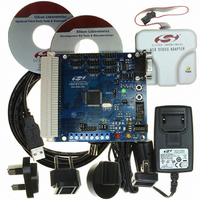
... All the peripherals (except for the ADC and SMBus) are stalled when the MCU is halted, during single stepping breakpoint in order to keep them synchronized. The C8051F120DK development kit provides all the hardware and software necessary to develop applica- tion code and perform in-circuit debugging with the C8051F12x or C8051F13x MCUs. ...
Page 31
MAC (Multiply and Accumulate) Engine The C8051F120/1/2/3 and C8051F130/1/2/3 devices include a multiply and accumulate engine which can be used to speed up many mathematical operations. MAC0 contains a 16-by-16 bit multiplier and a 40-bit adder, ...
Page 32
C8051F120/1/2/3/4/5/6/7 C8051F130/1/2/3 1.5. Programmable Digital I/O and Crossbar The standard 8051 8-bit Ports ( and 3) are available on the MCUs. The devices in the larger (100- pin TQFP) packaging have 4 additional ports ( and ...
Page 33
Programmable Counter Array An on-board Programmable Counter/Timer Array (PCA) is included in addition to the five 16-bit general purpose counter/timers. The PCA consists of a dedicated 16-bit counter/timer time base with 6 program- mable capture/compare modules. The timebase is ...
Page 34
C8051F120/1/2/3/4/5/6/7 C8051F130/1/2/3 1. 10-Bit Analog to Digital Converter All devices include either 10-bit SAR ADC (ADC0) with a 9-channel input multiplexer and program- mable gain amplifier. With a maximum throughput of 100 ksps, the 12 ...
Page 35
Analog to Digital Converter The C8051F12x devices have an on-board 8-bit SAR ADC (ADC2) with an 8-channel input multiplexer and programmable gain amplifier. This ADC features a 500 ksps maximum throughput and true 8-bit linearity with an INL ...
Page 36
C8051F120/1/2/3/4/5/6/7 C8051F130/1/2/3 1.10. 12-bit Digital to Analog Converters The C8051F12x devices have two integrated 12-bit Digital to Analog Converters (DACs). The MCU data and control interface to each DAC is via the Special Function Registers. The MCU can place either ...
Page 37
Analog Comparators Two analog comparators with dedicated input pins are included on-chip. The comparators have software programmable hysteresis and response time. Each comparator can generate an interrupt on a rising edge, falling edge, or both. The interrupts are capable ...
Page 38
C8051F120/1/2/3/4/5/6/7 C8051F130/1/2/3 2. Absolute Maximum Ratings Table 2.1. Absolute Maximum Ratings Parameter Ambient temperature under bias Storage Temperature Voltage on any Pin (except V and Port I/O) with DD Respect to DGND Voltage on any Port I/O Pin or RST ...
Page 39
Global DC Electrical Characteristics Table 3.1. Global DC Electrical Characteristics (C8051F120/1/2/3 and C8051F130/1/2/3) –40 to +85 °C, 100 MHz System Clock unless otherwise specified. Parameter 1 SYSCLK = MHz Analog Supply Voltage SYSCLK > 50 MHz ...
Page 40
C8051F120/1/2/3/4/5/6/7 C8051F130/1/2/3 Table 3.2. Global DC Electrical Characteristics (C8051F124/5/6/7) –40 to +85 °C, 50 MHz System Clock unless otherwise specified. Parameter 1 Analog Supply Voltage Analog Supply Current Internal REF, ADC, DAC, Com- parators all active Analog Supply Current with ...
Page 41
Pinout and Package Definitions Pin Numbers ‘F120 ‘F121 ‘F130 Name ‘F122 ‘F123 ‘F132 ‘F124 ‘F125 ‘F126 ‘F127 V 37, 24, DD 64, 90 41, 57 64, 90 DGND 38, 25, 63, 89 40, 56 63, 89 AV+ 11, 14 ...
Page 42
C8051F120/1/2/3/4/5/6/7 C8051F130/1/2/3 Table 4.1. Pin Definitions (Continued) Pin Numbers ‘F120 ‘F121 ‘F130 Name ‘F122 ‘F123 ‘F132 ‘F124 ‘F125 ‘F126 ‘F127 VREF 12 7 VREFA 8 VREF0 16 VREF2 17 VREFD 15 AIN0 AIN0 AIN0 ...
Page 43
Table 4.1. Pin Definitions (Continued) Pin Numbers ‘F120 ‘F121 ‘F130 Name ‘F122 ‘F123 ‘F132 ‘F124 ‘F125 ‘F126 ‘F127 DAC1 ...
Page 44
C8051F120/1/2/3/4/5/6/7 C8051F130/1/2/3 Table 4.1. Pin Definitions (Continued) Pin Numbers ‘F120 ‘F121 ‘F130 Name ‘F122 ‘F123 ‘F132 ‘F124 ‘F125 ‘F126 ‘F127 AIN2.2/A10/P1 AIN2.3/A11/P1 AIN2.4/A12/P1 AIN2.5/A13/P1 AIN2.6/A14/P1 AIN2.7/A15/P1 A8m/A0/P2.0 46 ...
Page 45
Table 4.1. Pin Definitions (Continued) Pin Numbers ‘F120 ‘F121 ‘F130 Name ‘F122 ‘F123 ‘F132 ‘F124 ‘F125 ‘F126 ‘F127 AD0/D0/P3 AD1/D1/P3 AD2/D2/P3 AD3/D3/P3 AD4/D4/P3 AD5/D5/P3.5 49 ...
Page 46
C8051F120/1/2/3/4/5/6/7 C8051F130/1/2/3 Table 4.1. Pin Definitions (Continued) Pin Numbers ‘F120 ‘F121 ‘F130 Name ‘F122 ‘F123 ‘F132 ‘F124 ‘F125 ‘F126 ‘F127 ALE/P4.5 93 RD/P4.6 92 WR/P4.7 91 A8/P5.0 88 A9/P5.1 87 A10/P5.2 86 A11/P5.3 85 A12/P5.4 84 A13/P5.5 83 A14/P5.6 82 ...
Page 47
Table 4.1. Pin Definitions (Continued) Pin Numbers ‘F120 ‘F121 ‘F130 Name ‘F122 ‘F123 ‘F132 ‘F124 ‘F125 ‘F126 ‘F127 A8m/A0/P6 A9m/A1/P6 A10m/A2/P6 A11m/A3/P6 A12m/A4/P6 A13m/A5/P6 A14m/A6/P6 A15m/A7/P6.7 ...
Page 48
C8051F120/1/2/3/4/5/6/7 C8051F130/1/2/3 Table 4.1. Pin Definitions (Continued) Pin Numbers ‘F120 ‘F121 ‘F130 Name ‘F122 ‘F123 ‘F132 ‘F124 ‘F125 ‘F126 ‘F127 AD5/D5/P7.5 67 AD6/D6/P7.6 66 AD7/D7/P7 100 48 ‘F131 Type ‘F133 67 D I/O Port 7.5. See Port Input/Output ...
Page 49
TMS 1 TCK 2 TDI 3 TDO 4 /RST 5 CP1- 6 CP1+ 7 CP0- 8 CP0+ 9 AGND 10 AV+ 11 VREF 12 AGND 13 AV+ 14 VREFD 15 VREF0 16 VREF2 17 AIN0.0 18 AIN0.1 19 AIN0.2 20 ...
Page 50
C8051F120/1/2/3/4/5/6/7 C8051F130/1/2/3 TMS 1 TCK 2 TDI 3 TDO 4 /RST 5 CP1- 6 CP1+ 7 CP0- 8 CP0+ 9 AGND 10 AV+ 11 VREF 12 AGND 13 AV VREF0 AIN0.0 18 AIN0.1 19 ...
Page 51
PIN 1 DESIGNATOR Figure 4.3. TQFP-100 Package Drawing C8051F120/1/2/3/4/5/6/7 C8051F130/1/2 Rev. 1.4 MIN NOM MAX (mm) (mm) (mm 1.20 A1 0.05 - 0.15 A2 0.95 1.00 ...
Page 52
C8051F120/1/2/3/4/5/6/7 C8051F130/1/2/3 CP1- 1 CP1+ 2 CP0- 3 CP0+ 4 AGND 5 AV+ 6 VREF 7 VREFA 8 AIN0.0 9 AIN0.1 10 AIN0.2 11 AIN0.3 12 AIN0.4 13 AIN0.5 14 AIN0.6 15 AIN0.7 16 Figure 4.4. C8051F121/3/5/7 Pinout Diagram (TQFP-64) ...
Page 53
CP1- 1 CP1+ 2 CP0- 3 CP0+ 4 AGND 5 AV+ 6 VREF 7 VREF0 8 AIN0.0 9 AIN0.1 10 AIN0.2 11 AIN0.3 12 AIN0.4 13 AIN0.5 14 AIN0.6 15 AIN0.7 16 Figure 4.5. C8051F131/3 Pinout Diagram (TQFP-64) C8051F120/1/2/3/4/5/6/7 C8051F130/1/2/3 ...
Page 54
C8051F120/1/2/3/4/5/6/7 C8051F130/1/2 PIN 1 DESIGNATOR Figure 4.6. TQFP-64 Package Drawing Rev. 1.4 MIN NOM MAX (mm) (mm) (mm 1.20 A1 0.05 - 0.15 A2 ...
Page 55
ADC0 (12-Bit ADC, C8051F120/1/4/5 Only) The ADC0 subsystem for the C8051F120/1/4/5 consists of a 9-channel, configurable analog multiplexer (AMUX0), a programmable gain amplifier (PGA0), and a 100 ksps, 12-bit successive-approximation-regis- ter ADC with integrated track-and-hold and Programmable Window Detector ...
Page 56
C8051F120/1/2/3/4/5/6/7 C8051F130/1/2/3 The Temperature Sensor transfer function is shown in Figure 5.2. The output voltage (V input when the Temperature Sensor is selected by bits AMX0AD3-0 in register AMX0SL; this voltage will be amplified by the PGA according to the ...
Page 57
ADC Modes of Operation ADC0 has a maximum conversion speed of 100 ksps. The ADC0 conversion clock is derived from the sys- tem clock divided by the value held in the ADCSC bits of register ADC0CF. 5.2.1. Starting a ...
Page 58
C8051F120/1/2/3/4/5/6/7 C8051F130/1/2/3 5.2.2. Tracking Modes The AD0TM bit in register ADC0CN controls the ADC0 track-and-hold mode. In its default state, the ADC0 input is continuously tracked when a conversion is not in progress. When the AD0TM bit is logic 1, ...
Page 59
Settling Time Requirements A minimum tracking time is required before an accurate conversion can be performed. This tracking time is determined by the ADC0 MUX resistance, the ADC0 sampling capacitance, any external source resis- tance, and the accuracy required ...
Page 60
C8051F120/1/2/3/4/5/6/7 C8051F130/1/2/3 SFR Definition 5.1. AMX0CF: AMUX0 Configuration 0 SFR Page: 0xBA SFR Address: R/W R/W R Bit7 Bit6 Bit5 Bits7–4: UNUSED. Read = 0000b; Write = don’t care. Bit3: AIN67IC: AIN0.6, AIN0.7 Input Pair Configuration Bit. ...
Page 61
SFR Definition 5.2. AMX0SL: AMUX0 Channel Select 0 SFR Page: 0xBB SFR Address: R/W R/W R Bit7 Bit6 Bit5 Bits7–4: UNUSED. Read = 0000b; Write = don’t care. Bits3–0: AMX0AD3–0: AMX0 Address Bits. 0000-1111b: ADC Inputs selected ...
Page 62
C8051F120/1/2/3/4/5/6/7 C8051F130/1/2/3 SFR Definition 5.3. ADC0CF: ADC0 Configuration 0 SFR Page: 0xBC SFR Address: R/W R/W R/W AD0SC4 AD0SC3 AD0SC2 Bit7 Bit6 Bit5 Bits7–3: AD0SC4–0: ADC0 SAR Conversion Clock Period Bits. The SAR Conversion clock is derived from system clock ...
Page 63
SFR Definition 5.4. ADC0CN: ADC0 Control 0 SFR Page: 0xE8 (bit addressable) SFR Address: R/W R/W R/W AD0EN AD0TM AD0INT AD0BUSY AD0CM1 AD0CM0 Bit7 Bit6 Bit5 Bit7: AD0EN: ADC0 Enable Bit. 0: ADC0 Disabled. ADC0 is in low-power shutdown. 1: ...
Page 64
C8051F120/1/2/3/4/5/6/7 C8051F130/1/2/3 SFR Definition 5.5. ADC0H: ADC0 Data Word MSB 0 SFR Page: 0xBF SFR Address: R/W R/W R/W Bit7 Bit6 Bit5 Bits7–0: ADC0 Data Word High-Order Bits. For AD0LJST = 0: Bits 7–4 are the sign extension of Bit3. ...
Page 65
ADC0 Data Word appears in the ADC0 Data Word Registers as follows: ADC0H[3:0]:ADC0L[7:0], if AD0LJST = 0 (ADC0H[7:4] will be sign-extension of ADC0H.3 for a differential reading, otherwise = 0000b). ADC0H[7:0]:ADC0L[7:4], if AD0LJST = 1 (ADC0L[3:0] = 0000b). Example: ...
Page 66
C8051F120/1/2/3/4/5/6/7 C8051F130/1/2/3 5.3. ADC0 Programmable Window Detector The ADC0 Programmable Window Detector continuously compares the ADC0 output to user-programmed limits, and notifies the system when an out-of-bound condition is detected. This is especially effective in an interrupt-driven system, saving code ...
Page 67
SFR Definition 5.9. ADC0LTH: ADC0 Less-Than Data High Byte 0 SFR Page: 0xC7 SFR Address: R/W R/W R/W Bit7 Bit6 Bit5 Bits7–0: High byte of ADC0 Less-Than Data Word. SFR Definition 5.10. ADC0LTL: ADC0 Less-Than Data Low Byte 0 SFR ...
Page 68
C8051F120/1/2/3/4/5/6/7 C8051F130/1/2/3 Input Voltage ADC Data (AD0.0 - AGND) Word REF x (4095/4096) 0x0FFF AD0WINT not affected 0x0201 REF x (512/4096) 0x0200 ADC0LTH:ADC0LTL 0x01FF AD0WINT=1 0x0101 REF x (256/4096) 0x0100 ADC0GTH:ADC0GTL 0x00FF AD0WINT not affected 0x0000 0 Given: AMX0SL = ...
Page 69
Input Voltage ADC Data (AD0.0 - AD0.1) Word REF x (2047/2048) 0x07FF AD0WINT not affected 0x0101 REF x (256/2048) 0x0100 ADC0LTH:ADC0LTL 0x00FF AD0WINT=1 0x0000 REF x (-1/2048) 0xFFFF ADC0GTH:ADC0GTL 0xFFFE AD0WINT not affected 0xF800 -REF Given: AMX0SL = 0x00, AMX0CF ...
Page 70
C8051F120/1/2/3/4/5/6/7 C8051F130/1/2/3 Input Voltage ADC Data (AD0.0 - AGND) Word REF x (4095/4096) 0xFFF0 AD0WINT not affected 0x2010 REF x (512/4096) 0x2000 ADC0LTH:ADC0LTL 0x1FF0 AD0WINT=1 0x1010 REF x (256/4096) 0x1000 ADC0GTH:ADC0GTL 0x0FF0 AD0WINT not affected 0x0000 0 Given: AMX0SL = ...
Page 71
Input Voltage ADC Data (AD0.0 - AD0.1) Word REF x (2047/2048) 0x7FF0 AD0WINT not affected 0x1010 REF x (256/2048) 0x1000 ADC0LTH:ADC0LTL 0x0FF0 AD0WINT=1 0x0000 REF x (-1/2048) 0xFFF0 ADC0GTH:ADC0GTL 0xFFE0 AD0WINT not affected 0x8000 -REF Given: AMX0SL = 0x00, AMX0CF ...
Page 72
C8051F120/1/2/3/4/5/6/7 C8051F130/1/2/3 Table 5.1. 12-Bit ADC0 Electrical Characteristics (C8051F120/1/4/ 3.0 V, AV+ = 3.0 V, VREF = 2.40 V (REFBE = 0), PGA Gain = 1, –40 to +85 °C unless otherwise specified. DD Parameter Resolution Integral Nonlinearity ...
Page 73
ADC0 (10-Bit ADC, C8051F122/3/6/7 and C8051F13x Only) The ADC0 subsystem for the C8051F122/3/6/7 and C8051F13x consists of a 9-channel, configurable ana- log multiplexer (AMUX0), a programmable gain amplifier (PGA0), and a 100 ksps, 10-bit successive- approximation-register ADC with integrated ...
Page 74
C8051F120/1/2/3/4/5/6/7 C8051F130/1/2/3 The Temperature Sensor transfer function is shown in Figure 6.2. The output voltage (V input when the Temperature Sensor is selected by bits AMX0AD3-0 in register AMX0SL; this voltage will be amplified by the PGA according to the ...
Page 75
ADC Modes of Operation ADC0 has a maximum conversion speed of 100 ksps. The ADC0 conversion clock is derived from the sys- tem clock divided by the value held in the ADCSC bits of register ADC0CF. 6.2.1. Starting a ...
Page 76
C8051F120/1/2/3/4/5/6/7 C8051F130/1/2/3 6.2.2. Tracking Modes The AD0TM bit in register ADC0CN controls the ADC0 track-and-hold mode. In its default state, the ADC0 input is continuously tracked when a conversion is not in progress. When the AD0TM bit is logic 1, ...
Page 77
Settling Time Requirements A minimum tracking time is required before an accurate conversion can be performed. This tracking time is determined by the ADC0 MUX resistance, the ADC0 sampling capacitance, any external source resis- tance, and the accuracy required ...
Page 78
C8051F120/1/2/3/4/5/6/7 C8051F130/1/2/3 SFR Definition 6.1. AMX0CF: AMUX0 Configuration 0 SFR Page: 0xBA SFR Address: R/W R/W R Bit7 Bit6 Bit5 Bits7–4: UNUSED. Read = 0000b; Write = don’t care. Bit3: AIN67IC: AIN0.6, AIN0.7 Input Pair Configuration Bit. ...
Page 79
SFR Definition 6.2. AMX0SL: AMUX0 Channel Select 0 SFR Page: 0xBB SFR Address: R/W R/W R Bit7 Bit6 Bit5 Bits7–4: UNUSED. Read = 0000b; Write = don’t care. Bits3–0: AMX0AD3–0: AMX0 Address Bits. 0000-1111b: ADC Inputs selected ...
Page 80
C8051F120/1/2/3/4/5/6/7 C8051F130/1/2/3 SFR Definition 6.3. ADC0CF: ADC0 Configuration 0 SFR Page: 0xBC SFR Address: R/W R/W R/W AD0SC4 AD0SC3 AD0SC2 Bit7 Bit6 Bit5 Bits7–3: AD0SC4–0: ADC0 SAR Conversion Clock Period Bits. SAR Conversion clock is derived from system clock by ...
Page 81
SFR Definition 6.4. ADC0CN: ADC0 Control 0 SFR Page: 0xE8 (bit addressable) SFR Address: R/W R/W R/W AD0EN AD0TM AD0INT AD0BUSY AD0CM1 AD0CM0 Bit7 Bit6 Bit5 Bit7: AD0EN: ADC0 Enable Bit. 0: ADC0 Disabled. ADC0 is in low-power shutdown. 1: ...
Page 82
C8051F120/1/2/3/4/5/6/7 C8051F130/1/2/3 SFR Definition 6.5. ADC0H: ADC0 Data Word MSB 0 SFR Page: 0xBF SFR Address: R/W R/W R/W Bit7 Bit6 Bit5 Bits7–0: ADC0 Data Word High-Order Bits. For AD0LJST = 0: Bits 7–4 are the sign extension of Bit3. ...
Page 83
ADC0 Data Word appears in the ADC0 Data Word Registers as follows: ADC0H[1:0]:ADC0L[7:0], if AD0LJST = 0 (ADC0H[7:2] will be sign-extension of ADC0H.1 for a differential reading, otherwise = 000000b). ADC0H[7:0]:ADC0L[7:6], if AD0LJST = 1 (ADC0L[5:0] = 00b). Example: ...
Page 84
C8051F120/1/2/3/4/5/6/7 C8051F130/1/2/3 6.3. ADC0 Programmable Window Detector The ADC0 Programmable Window Detector continuously compares the ADC0 output to user-programmed limits, and notifies the system when an out-of-bound condition is detected. This is especially effective in an interrupt-driven system, saving code ...
Page 85
SFR Definition 6.9. ADC0LTH: ADC0 Less-Than Data High Byte 0 SFR Page: 0xC7 SFR Address: R/W R/W R/W Bit7 Bit6 Bit5 Bits7–0: High byte of ADC0 Less-Than Data Word. SFR Definition 6.10. ADC0LTL: ADC0 Less-Than Data Low Byte 0 SFR ...
Page 86
C8051F120/1/2/3/4/5/6/7 C8051F130/1/2/3 Input Voltage ADC Data (AD0.0 - AGND) Word REF x (1023/1024) 0x03FF ADWINT not affected 0x0201 REF x (512/1024) 0x0200 ADC0LTH:ADC0LTL 0x01FF ADWINT=1 0x0101 REF x (256/1024) 0x0100 ADC0GTH:ADC0GTL 0x00FF ADWINT not affected 0x0000 0 Given: AMX0SL = ...
Page 87
Input Voltage ADC Data (AD0.0 - AD0.1) Word REF x (511/512) 0x01FF ADWINT not affected 0x0101 REF x (256/512) 0x0100 ADC0LTH:ADC0LTL 0x00FF ADWINT=1 0x0000 REF x (-1/512) 0xFFFF ADC0GTH:ADC0GTL 0xFFFE ADWINT not affected 0xFE00 -REF Given: AMX0SL = 0x00, AMX0CF ...
Page 88
C8051F120/1/2/3/4/5/6/7 C8051F130/1/2/3 Input Voltage ADC Data (AD0.0 - AGND) Word REF x (1023/1024) 0xFFC0 ADWINT not affected 0x8040 REF x (512/1024) 0x8000 ADC0LTH:ADC0LTL 0x7FC0 ADWINT=1 0x4040 REF x (256/1024) 0x4000 ADC0GTH:ADC0GTL 0x3FC0 ADWINT not affected 0x0000 0 Given: AMX0SL = ...
Page 89
Input Voltage ADC Data (AD0.0 - AD0.1) Word REF x (511/512) 0x7FC0 ADWINT not affected 0x2040 REF x (128/512) 0x2000 ADC0LTH:ADC0LTL 0x1FC0 ADWINT=1 0x0000 REF x (-1/512) 0xFFC0 ADC0GTH:ADC0GTL 0xFF80 ADWINT not affected 0x8000 -REF Given: AMX0SL = 0x00, AMX0CF ...
Page 90
C8051F120/1/2/3/4/5/6/7 C8051F130/1/2/3 Table 6.1. 10-Bit ADC0 Electrical Characteristics (C8051F122/3/6/7 and C8051F13x 3.0 V, AV+ = 3.0 V, VREF = 2.40 V (REFBE = 0), PGA Gain = 1, –40 to +85 °C unless otherwise specified. DD Parameter Resolution ...
Page 91
ADC2 (8-Bit ADC, C8051F12x Only) The C8051F12x devices include a second ADC peripheral (ADC2), which consists of an 8-channel, config- urable analog multiplexer, a programmable gain amplifier, and a 500 ksps, 8-bit successive-approximation- register ADC with integrated track-and-hold (see ...
Page 92
C8051F120/1/2/3/4/5/6/7 C8051F130/1/2/3 7.2. ADC2 Modes of Operation ADC2 has a maximum conversion speed of 500 ksps. The ADC2 conversion clock (SAR2 clock divided version of the system clock, determined by the AD2SC bits in the ADC2CF register. The ...
Page 93
A. ADC Timing for External Trigger Source CNVSTR2 (AD2CM[2:0]=010) SAR Clocks Low Power AD2TM=1 or Convert AD2TM=0 Track or Convert B. ADC Timing for Internal Trigger Source Write '1' to AD2BUSY, Timer 3 Overflow, Timer 2 Overflow, Write '1' to ...
Page 94
C8051F120/1/2/3/4/5/6/7 C8051F130/1/2/3 7.2.3. Settling Time Requirements A minimum tracking time is required before an accurate conversion can be performed. This tracking time is determined by the ADC2 MUX resistance, the ADC2 sampling capacitance, any external source resis- tance, and the ...
Page 95
SFR Definition 7.1. AMX2CF: AMUX2 Configuration 2 SFR Page: 0xBA SFR Address: R/W R/W R Bit7 Bit6 Bit5 Bits7–4: UNUSED. Read = 0000b; Write = don’t care. Bit3: PIN67IC: AIN2.6, AIN2.7 Input Pair Configuration Bit. 0: AIN2.6 ...
Page 96
C8051F120/1/2/3/4/5/6/7 C8051F130/1/2/3 SFR Definition 7.2. AMX2SL: AMUX2 Channel Select 2 SFR Page: 0xBB SFR Address: R/W R/W R Bit7 Bit6 Bit5 Bits7–3: UNUSED. Read = 00000b; Write = don’t care. Bits2–0: AMX2AD2–0: AMX2 Address Bits. 000-111b: ADC ...
Page 97
SFR Definition 7.3. ADC2CF: ADC2 Configuration 2 SFR Page: 0xBC SFR Address: R/W R/W R/W AD2SC4 AD2SC3 AD2SC2 Bit7 Bit6 Bit5 Bits7–3: AD2SC4–0: ADC2 SAR Conversion Clock Period Bits. SAR Conversion clock is derived from system clock by the following ...
Page 98
C8051F120/1/2/3/4/5/6/7 C8051F130/1/2/3 SFR Definition 7.4. ADC2CN: ADC2 Control 2 SFR Page: 0xE8 (bit addressable) SFR Address: R/W R/W R/W AD2EN AD2TM AD2INT AD2BUSY AD2CM2 AD2CM1 Bit7 Bit6 Bit5 Bit7: AD2EN: ADC2 Enable Bit. 0: ADC2 Disabled. ADC2 is in low-power ...
Page 99
SFR Definition 7.5. ADC2: ADC2 Data Word 2 SFR Page: 0xBE SFR Address: R/W R/W R/W Bit7 Bit6 Bit5 Bits7–0: ADC2 Data Word. Single-Ended Example: 8-bit ADC Data Word appears in the ADC2 Data Word Register as follows: Example: ADC2 ...
Page 100
C8051F120/1/2/3/4/5/6/7 C8051F130/1/2/3 7.3. ADC2 Programmable Window Detector The ADC2 Programmable Window Detector continuously compares the ADC2 output to user-programmed limits, and notifies the system when a desired condition is detected. This is especially effective in an inter- rupt-driven system, saving ...
Page 101
Window Detector In Differential Mode Figure 7.6 shows two example window comparisons for differential mode, with ADC2LT = 0x10 (+16d) and ADC2GT = 0xFF (-1d). Notice that in Differential mode, the codes vary from -VREF to VREF*(127/128) and are ...
Page 102
C8051F120/1/2/3/4/5/6/7 C8051F130/1/2/3 SFR Definition 7.6. ADC2GT: ADC2 Greater-Than Data Byte 2 SFR Page: 0xC4 SFR Address: R/W R/W R/W Bit7 Bit6 Bit5 Bits7–0: ADC2 Greater-Than Data Word. SFR Definition 7.7. ADC2LT: ADC2 Less-Than Data Byte 2 SFR Page: 0xC6 SFR ...
Page 103
Table 7.1. ADC2 Electrical Characteristics V = 3.0 V, AV+ = 3.0 V, VREF2 = 2.40 V (REFBE = 0), PGA gain = 1, –40 to +85 °C unless otherwise specified. DD Parameter Resolution Integral Nonlinearity Differential Nonlinearity Guaranteed Monotonic ...
Page 104
C8051F120/1/2/3/4/5/6/7 C8051F130/1/2 OTES 104 Rev. 1.4 ...
Page 105
DACs, 12-Bit Voltage Mode (C8051F12x Only) The C8051F12x devices include two on-chip 12-bit voltage-mode Digital-to-Analog Converters (DACs). Each DAC has an output swing (VREF-1LSB) for a corresponding input code range of 0x000 to 0xFFF. The ...
Page 106
C8051F120/1/2/3/4/5/6/7 C8051F130/1/2/3 8.1.1. Update Output On-Demand In its default mode (DAC0CN.[4:3] = ‘00’) the DAC0 output is updated “on-demand” write to the high- byte of the DAC0 data register (DAC0H important to note that writes to ...
Page 107
SFR Definition 8.1. DAC0H: DAC0 High Byte R/W R/W R/W Bit7 Bit6 Bit5 Bits7–0: DAC0 Data Word Most Significant Byte. SFR Definition 8.2. DAC0L: DAC0 Low Byte R/W R/W R/W Bit7 Bit6 Bit5 Bits7–0: DAC0 Data Word Least Significant Byte. ...
Page 108
C8051F120/1/2/3/4/5/6/7 C8051F130/1/2/3 SFR Definition 8.3. DAC0CN: DAC0 Control R/W R/W R/W DAC0EN - - Bit7 Bit6 Bit5 Bit7: DAC0EN: DAC0 Enable Bit. 0: DAC0 Disabled. DAC0 Output pin is disabled; DAC0 is in low-power shutdown mode. 1: DAC0 Enabled. DAC0 ...
Page 109
SFR Definition 8.4. DAC1H: DAC1 High Byte R/W R/W R/W Bit7 Bit6 Bit5 Bits7–0: DAC1 Data Word Most Significant Byte. SFR Definition 8.5. DAC1L: DAC1 Low Byte R/W R/W R/W Bit7 Bit6 Bit5 Bits7–0: DAC1 Data Word Least Significant Byte. ...
Page 110
C8051F120/1/2/3/4/5/6/7 C8051F130/1/2/3 SFR Definition 8.6. DAC1CN: DAC1 Control R/W R/W R/W DAC1EN - - Bit7 Bit6 Bit5 Bit7: DAC1EN: DAC1 Enable Bit. 0: DAC1 Disabled. DAC1 Output pin is disabled; DAC1 is in low-power shutdown mode. 1: DAC1 Enabled. DAC1 ...
Page 111
Table 8.1. DAC Electrical Characteristics V = 3.0 V, AV+ = 3.0 V, VREF = 2.40 V (REFBE = 0), No Output Load unless otherwise specified DD Parameter Resolution Integral Nonlinearity Differential Nonlinearity No Output Filter Output Noise 100 ...
Page 112
C8051F120/1/2/3/4/5/6/7 C8051F130/1/2 OTES 112 Rev. 1.4 ...
Page 113
Voltage Reference The voltage reference options available on the C8051F12x and C8051F13x device families vary according to the device capabilities. All devices include an internal voltage reference circuit, consisting ppm/°C (typical) bandgap voltage reference ...
Page 114
C8051F120/1/2/3/4/5/6/7 C8051F130/1/2/3 VDD External R1 Voltage Reference Circuit DGND + 4.7F 0.1F Recommended Bypass Capacitors Figure 9.1. Voltage Reference Functional Block Diagram (C8051F120/2/4/6) SFR Definition 9.1. REF0CN: Reference Control (C8051F120/2/4/6) 0 SFR Page: 0xD1 SFR Address: R/W R/W R/W - ...
Page 115
Reference Configuration on the C8051F121/3/5/7 On the C8051F121/3/5/7 devices, the REF0CN register also allows selection of the voltage reference source for ADC0 and ADC2, as shown in SFR Definition 9.2. Bits AD0VRS and AD2VRS in the REF0CN register select ...
Page 116
C8051F120/1/2/3/4/5/6/7 C8051F130/1/2/3 SFR Definition 9.2. REF0CN: Reference Control (C8051F121/3/5/7) 0 SFR Page: 0xD1 SFR Address: R/W R/W R Bit7 Bit6 Bit5 Bits7–5: UNUSED. Read = 000b; Write = don’t care. Bit4: AD0VRS: ADC0 Voltage Reference Select. 0: ...
Page 117
Reference Configuration on the C8051F130/1/2/3 On the C8051F130/1/2/3 devices, the VREF0 pin provides a voltage reference input for ADC0, which can be connected to an external precision reference or the internal voltage reference, as shown in Figure 9.3. The ...
Page 118
C8051F120/1/2/3/4/5/6/7 C8051F130/1/2/3 Table 9.1. Voltage Reference Electrical Characteristics V = 3.0 V, AV+ = 3.0 V, –40 to +85 °C unless otherwise specified. DD Parameter Analog Bias Generator Power BIASE = 1 Supply Current Output Voltage 25 °C ambient VREF ...
Page 119
Comparators Two on-chip programmable voltage comparators are included, as shown in Figure 10.1. The inputs of each comparator are available at dedicated pins. The output of each comparator is optionally available at the package pins via the I/O crossbar. ...
Page 120
C8051F120/1/2/3/4/5/6/7 C8051F130/1/2/3 Comparator interrupts can be generated on rising-edge and/or falling-edge output transitions. (For inter- rupt enable and priority control, see set upon a Comparator0 falling-edge interrupt, and the CP0RIF flag is set upon the Comparator0 rising- edge interrupt. Once ...
Page 121
CP0+ VIN+ + CP0 CP0- _ VIN- CIRCUIT CONFIGURATION Positive Hysteresis Voltage (Programmed with CP0HYP Bits) VIN- INPUTS VIN OUTPUT V OL Positive Hysteresis Disabled Positive Hysteresis Figure 10.2. Comparator Hysteresis Plot C8051F120/1/2/3/4/5/6/7 C8051F130/1/2/3 OUT (Programmed by CP0HYN ...
Page 122
C8051F120/1/2/3/4/5/6/7 C8051F130/1/2/3 SFR Definition 10.1. CPT0CN: Comparator0 Control 1 SFR Page: 0x88 SFR Address: R/W R/W R/W CP0EN CP0OUT CP0RIF Bit7 Bit6 Bit5 Bit7: CP0EN: Comparator0 Enable Bit. 0: Comparator0 Disabled. 1: Comparator0 Enabled. Bit6: CP0OUT: Comparator0 Output State Flag. ...
Page 123
SFR Definition 10.2. CPT0MD: Comparator0 Mode Selection 1 SFR Page: 0x89 SFR Address: R/W R/W R CP0RIE Bit7 Bit6 Bit5 Bits7–6: UNUSED. Read = 00b, Write = don’t care. Bit 5: CP0RIE: Comparator 0 Rising-Edge Interrupt Enable Bit. ...
Page 124
C8051F120/1/2/3/4/5/6/7 C8051F130/1/2/3 SFR Definition 10.3. CPT1CN: Comparator1 Control 2 SFR Page: 0x88 SFR Address: R/W R/W R/W CP1EN CP1OUT CP1RIF Bit7 Bit6 Bit5 Bit7: CP1EN: Comparator1 Enable Bit. 0: Comparator1 Disabled. 1: Comparator1 Enabled. Bit6: CP1OUT: Comparator1 Output State Flag. ...
Page 125
SFR Definition 10.4. CPT1MD: Comparator1 Mode Selection 2 SFR Page: 0x89 SFR Address: R/W R/W R CP1RIE Bit7 Bit6 Bit5 Bits7–6: UNUSED. Read = 00b, Write = don’t care. Bit 5: CP1RIE: Comparator 1 Rising-Edge Interrupt Enable Bit. ...
Page 126
C8051F120/1/2/3/4/5/6/7 C8051F130/1/2/3 Table 10.1. Comparator Electrical Characteristics V = 3.0 V, AV+ = 3.0 V, –40 to +85 °C unless otherwise specified. DD Parameter Response Time: * Mode 1 Response Time: * Mode 1, V ...
Page 127
CIP-51 Microcontroller The MCU system controller core is the CIP-51 microcontroller. The CIP-51 is fully compatible with the MCS-51™ instruction set; standard 803x/805x assemblers and compilers can be used to develop soft- ware. The MCU family has a superset ...
Page 128
C8051F120/1/2/3/4/5/6/7 C8051F130/1/2/3 ACCUMULATOR PSW DATA POINTER PC INCREMENTER PROGRAM COUNTER (PC) PRGM. ADDRESS REG. CONTROL RESET LOGIC CLOCK STOP POWER CONTROL IDLE Figure 11.1. CIP-51 Block Diagram Programming and Debugging Support A JTAG-based serial interface is provided for in-system programming ...
Page 129
Instruction Set The instruction set of the CIP-51 System Controller is fully compatible with the standard MCS-51™ instruc- tion set; standard 8051 development tools can be used to develop software for the CIP-51. All CIP-51 instructions are the binary ...
Page 130
C8051F120/1/2/3/4/5/6/7 C8051F130/1/2/3 Table 11.1. CIP-51 Instruction Set Summary (Continued) Mnemonic Description DEC A Decrement A DEC Rn Decrement register DEC direct Decrement direct byte DEC @Ri Decrement indirect RAM INC DPTR Increment Data Pointer MUL AB Multiply A and B ...
Page 131
Table 11.1. CIP-51 Instruction Set Summary (Continued) Mnemonic Description MOV direct, @Ri Move indirect RAM to direct byte MOV direct, #data Move immediate to direct byte MOV @Ri, A Move A to indirect RAM MOV @Ri, direct Move direct byte ...
Page 132
C8051F120/1/2/3/4/5/6/7 C8051F130/1/2/3 Table 11.1. CIP-51 Instruction Set Summary (Continued) Mnemonic Description JZ rel Jump if A equals zero JNZ rel Jump if A does not equal zero CJNE A, direct, rel Compare direct byte to A and jump if not ...
Page 133
Memory Organization The memory organization of the CIP-51 System Controller is similar to that of a standard 8051. There are two separate memory spaces: program memory and data memory. Program and data memory share the same address space but ...
Page 134
C8051F120/1/2/3/4/5/6/7 C8051F130/1/2/3 SFR Definition 11.1. PSBANK: Program Space Bank Select R/W R/W R COBANK Bit7 Bit6 Bit5 Bits 7 – 6: Reserved. Bits 5 – 4: COBANK: Constant Operations Bank Select. These bits select which Flash bank is ...
Page 135
Data Memory The CIP-51 implements 256 bytes of internal RAM mapped into the data memory space from 0x00 through 0xFF. The lower 128 bytes of data memory are used for general purpose registers and memory. Either direct or indirect ...
Page 136
C8051F120/1/2/3/4/5/6/7 C8051F130/1/2/3 and a RET pops two record bits, also.) The stack record circuitry can also detect an overflow or underflow on the 32-bit shift register, and can notify the debug software even with the MCU running at speed. 11.2.6. ...
Page 137
Interrupt Logic CIP-51 Figure 11.4. SFR Page Stack Automatic hardware switching of the SFR Page on interrupts may be enabled or disabled as desired using the SFR Automatic Page Control Enable Bit located in the SFR Page Control Register (SFRPGCN). ...
Page 138
C8051F120/1/2/3/4/5/6/7 C8051F130/1/2/3 11.2.6.3.SFR Page Stack Example The following is an example that shows the operation of the SFR Page Stack during interrupts. In this example, the SFR Page Control is left in the default enabled state (i.e., SFRPGEN = 1), ...
Page 139
SFRPAGE pushed to SFRNEXT Figure 11.6. SFR Page Stack After ADC2 Window Comparator Interrupt Occurs While in the ADC2 ISR, a PCA interrupt occurs. Recall the PCA interrupt is configured as a high priority interrupt, while the ADC2 interrupt is ...
Page 140
C8051F120/1/2/3/4/5/6/7 C8051F130/1/2/3 SFRPAGE pushed to SFRNEXT SFRNEXT pushed to SFRLAST Figure 11.7. SFR Page Stack Upon PCA Interrupt Occurring During an ADC2 ISR On exit from the PCA interrupt service routine, the CIP-51 will return to the ADC2 Window Comparator ...
Page 141
On the execution of the RETI instruction in the ADC2 Window Comparator ISR, the value in SFRPAGE register is overwritten with the contents of SFRNEXT. The CIP-51 may now access the Port 5 SFR bits as it did prior to ...
Page 142
C8051F120/1/2/3/4/5/6/7 C8051F130/1/2/3 SFR Definition 11.2. SFRPGCN: SFR Page Control R/W R/W R Bit7 Bit6 Bit5 Bits7–1: Reserved. Bit0: SFRPGEN: SFR Automatic Page Control Enable. Upon interrupt, the C8051 Core will vector to the specified interrupt service routine ...
Page 143
SFR Definition 11.4. SFRNEXT: SFR Next Register R/W R/W R/W Bit7 Bit6 Bit5 Bits7–0: SFR Page Stack Bits: SFR page context is retained upon interrupts/return from interrupts byte SFR Page Stack: SFRPAGE is the first entry, SFRNEXT ...
Page 144
C8051F120/1/2/3/4/5/6/7 C8051F130/1/2/3 Table 11.2. Special Function Register (SFR) Memory Map 0(8) 1(9) 0 SPI0CN PCA0L PCA0H (ALL 3 PAGES ADC0CN PCA0CPL2 PCA0CPH2 PCA0CPL3 PCA0CPH3 PCA0CPL4 PCA0CPH4 1 ...
Page 145
Table 11.2. Special Function Register (SFR) Memory Map (Continued) 0 SADEN0 AMX0CF (ALL AMX2CF 3 PAGES PSBANK B0 2 (ALL (ALL 3 PAGES) PAGES SADDR0 (ALL ...
Page 146
C8051F120/1/2/3/4/5/6/7 C8051F130/1/2/3 Table 11.3. Special Function Registers SFRs are listed in alphabetical order. All undefined SFR locations are reserved. SFR Register Address Page ACC 0xE0 All Pages Accumulator ADC0CF 0xBC 0 ADC0CN 0xE8 0 ADC0GTH 0xC5 0 ADC0GTL 0xC4 0 ...
Page 147
Table 11.3. Special Function Registers (Continued) SFRs are listed in alphabetical order. All undefined SFR locations are reserved. SFR Register Address Page EIE1 0xE6 All Pages Extended Interrupt Enable 1 EIE2 0xE7 All Pages Extended Interrupt Enable 2 EIP1 0xF6 ...
Page 148
C8051F120/1/2/3/4/5/6/7 C8051F130/1/2/3 Table 11.3. Special Function Registers (Continued) SFRs are listed in alphabetical order. All undefined SFR locations are reserved. SFR Register Address Page P6 0xE8 F P6MDOUT 0x9E F P7 0xF8 F P7MDOUT 0x9F F PCA0CN 0xD8 0 PCA0CPH0 ...
Page 149
Table 11.3. Special Function Registers (Continued) SFRs are listed in alphabetical order. All undefined SFR locations are reserved. SFR Register Address Page REF0CN 0xD1 0 RSTSRC 0xEF 0 SADDR0 0xA9 0 SADEN0 0xB9 0 SBUF0 0x99 0 SBUF1 0x99 1 ...
Page 150
C8051F120/1/2/3/4/5/6/7 C8051F130/1/2/3 Table 11.3. Special Function Registers (Continued) SFRs are listed in alphabetical order. All undefined SFR locations are reserved. SFR Register Address Page TMR4L 0xCC 2 WDTCN 0xFF All Pages Watchdog Timer Control XBR0 0xE1 F XBR1 0xE2 F ...
Page 151
Register Descriptions Following are descriptions of SFRs related to the operation of the CIP-51 System Controller. Reserved bits should not be set to logic l. Future product versions may use these bits to implement new features in which case ...
Page 152
C8051F120/1/2/3/4/5/6/7 C8051F130/1/2/3 SFR Definition 11.9. PSW: Program Status Word R/W R/W R Bit7 Bit6 Bit5 Bit7: CY: Carry Flag. This bit is set when the last arithmetic operation resulted in a carry (addition borrow (subtraction). ...
Page 153
SFR Definition 11.10. ACC: Accumulator R/W R/W R/W ACC.7 ACC.6 ACC.5 Bit7 Bit6 Bit5 Bits7–0: ACC: Accumulator. This register is the accumulator for arithmetic operations. SFR Definition 11.11 Register R/W R/W R/W B.7 B.6 B.5 Bit7 Bit6 Bit5 ...
Page 154
C8051F120/1/2/3/4/5/6/7 C8051F130/1/2/3 11.3. Interrupt Handler The CIP-51 includes an extended interrupt system supporting a total of 20 interrupt sources with two prior- ity levels. The allocation of interrupt sources between on-chip peripherals and external input pins varies according to the ...
Page 155
External Interrupts Two of the external interrupt sources (/INT0 and /INT1) are configurable as active-low level-sensitive or active-low edge-sensitive inputs depending on the setting of bits IT0 (TCON.0) and IT1 (TCON.2). IE0 (TCON.1) and IE1 (TCON.3) serve as the ...
Page 156
C8051F120/1/2/3/4/5/6/7 C8051F130/1/2/3 Table 11.4. Interrupt Summary (Continued) Interru Interrupt Source pt Vector Comparator 1 Rising Edge 0x006B Timer 3 0x0073 ADC0 End of Conversion 0x007B Timer 4 0x0083 ADC2 Window Comparator 0x008B ADC2 End of Conversion 0x0093 RESERVED 0x009B UART1 ...
Page 157
Interrupt Register Descriptions The SFRs used to enable the interrupt sources and set their priority level are described below. Refer to the datasheet section associated with a particular on-chip peripheral for information regarding valid interrupt conditions for the peripheral ...
Page 158
C8051F120/1/2/3/4/5/6/7 C8051F130/1/2/3 SFR Definition 11.13. IP: Interrupt Priority R/W R/W R PT2 Bit7 Bit6 Bit5 Bits7–6: UNUSED. Read = 11b, Write = don't care. Bit5: PT2: Timer 2 Interrupt Priority Control. This bit sets the priority of the ...
Page 159
SFR Definition 11.14. EIE1: Extended Interrupt Enable 1 R/W R/W R/W ECP1R ECP1F ECP0R Bit7 Bit6 Bit5 Bit7: ECP1R: Enable Comparator1 (CP1) Rising Edge Interrupt. This bit sets the masking of the CP1 rising edge interrupt. 0: Disable CP1 rising ...
Page 160
C8051F120/1/2/3/4/5/6/7 C8051F130/1/2/3 SFR Definition 11.15. EIE2: Extended Interrupt Enable 2 R/W R/W R/W - ES1 - Bit7 Bit6 Bit5 Bit7: UNUSED. Read = 0b, Write = don't care. Bit6: ES1: Enable UART1 Interrupt. This bit sets the masking of the ...
Page 161
SFR Definition 11.16. EIP1: Extended Interrupt Priority 1 R/W R/W R/W PCP1R PCP1F PCP0R Bit7 Bit6 Bit5 Bit7: PCP1R: Comparator1 (CP1) Rising Interrupt Priority Control. This bit sets the priority of the CP1 interrupt. 0: CP1 rising interrupt set to ...
Page 162
C8051F120/1/2/3/4/5/6/7 C8051F130/1/2/3 SFR Definition 11.17. EIP2: Extended Interrupt Priority 2 R/W R/W R/W - PS1 - Bit7 Bit6 Bit5 Bit7: UNUSED. Read = 0b, Write = don't care. Bit6: ES1: UART1 Interrupt Priority Control. This bit sets the priority of ...
Page 163
Power Management Modes The CIP-51 core has two software programmable power management modes: Idle and Stop. Idle mode halts the CPU while leaving the external peripherals and internal clocks active. In Stop mode, the CPU is halted, all interrupts ...
Page 164
C8051F120/1/2/3/4/5/6/7 C8051F130/1/2/3 11.4.2. Stop Mode Setting the Stop Mode Select bit (PCON.1) causes the CIP-51 to enter Stop mode as soon as the instruc- tion that sets the bit completes. In Stop mode, the CPU and oscillators are stopped, effectively ...
Page 165
Multiply And Accumulate (MAC0) The C8051F120/1/2/3 and C8051F130/1/2/3 devices include a multiply and accumulate engine which can be used to speed up many mathematical operations. MAC0 contains a 16-by-16 bit multiplier and a 40-bit adder, which can perform integer ...
Page 166
C8051F120/1/2/3/4/5/6/7 C8051F130/1/2/3 12.2. Integer and Fractional Math MAC0 is capable of interpreting the 16-bit inputs stored in MAC0A and MAC0B as signed integers or as signed fractional numbers. When the MAC0FM bit (MAC0CF.1) is cleared to ‘0’, the inputs are ...
Page 167
Operating in Multiply and Accumulate Mode MAC0 operates in Multiply and Accumulate (MAC) mode when the MAC0MS bit (MAC0CF.0) is cleared to ‘0’. When operating in MAC mode, MAC0 performs a 16-by-16 bit multiply on the contents of the ...
Page 168
C8051F120/1/2/3/4/5/6/7 C8051F130/1/2/3 12.6. Rounding and Saturation A Rounding Engine is included, which can be used to provide a rounded result when operating on frac- tional numbers. MAC0 uses an unbiased rounding algorithm to round the data stored in bits 31 ...
Page 169
Multiply Only Example The example below implements the equation: MOV MAC0CF, #01h ; Use integer numbers, and multiply only mode (add to zero) MOV MAC0AH, #12h ; Load MAC0A register with 1234 hex = 4660 decimal MOV MAC0AL, #34h ...
Page 170
C8051F120/1/2/3/4/5/6/7 C8051F130/1/2/3 SFR Definition 12.1. MAC0CF: MAC0 Configuration MAC0SC MAC0SD MAC0CA MAC0SAT MAC0FM MAC0MS 00000000 Bit7 Bit6 Bit5 Bits 7 – 6: UNUSED: Read = 00b, Write = don’t care. Bit 5: MAC0SC: Accumulator Shift ...
Page 171
SFR Definition 12.2. MAC0STA: MAC0 Status Bit7 Bit6 Bit5 Bits 7 – 4: UNUSED: Read = 0000b, Write = don’t care. Bit 3: MAC0HO: Hard Overflow Flag. This bit is set to ‘1’ whenever ...
Page 172
C8051F120/1/2/3/4/5/6/7 C8051F130/1/2/3 SFR Definition 12.4. MAC0AL: MAC0 A Low Byte Bit7 Bit6 Bit5 Bits 7 – 0: Low Byte (bits 7 – MAC0 A Register. SFR Definition 12.5. MAC0BH: MAC0 B High Byte R R ...
Page 173
SFR Definition 12.7. MAC0ACC3: MAC0 Accumulator Byte Bit7 Bit6 Bit5 Bits 7 – 0: Byte 3 (bits 31 – 24) of MAC0 Accumulator. *Note: The contents of this register should not be changed by software during ...
Page 174
C8051F120/1/2/3/4/5/6/7 C8051F130/1/2/3 SFR Definition 12.10. MAC0ACC0: MAC0 Accumulator Byte Bit7 Bit6 Bit5 Bits 7 – 0: Byte 0 (bits 7 – MAC0 Accumulator. *Note: The contents of this register should not be changed by ...
Page 175
SFR Definition 12.13. MAC0RNDL: MAC0 Rounding Register Low Byte Bit7 Bit6 Bit5 Bits 7 – 0: Low Byte (bits 7 – MAC0 Rounding Register. C8051F120/1/2/3/4/5/6/7 C8051F130/1/2 Bit4 Bit3 Bit2 Bit1 Rev. ...
Page 176
C8051F120/1/2/3/4/5/6/7 C8051F130/1/2/3 176 Rev. 1.4 ...
Page 177
Reset Sources Reset circuitry allows the controller to be easily placed in a predefined default condition. On entry to this reset state, the following occur: • CIP-51 halts program execution. • Special Function Registers (SFRs) are initialized to their ...
Page 178
C8051F120/1/2/3/4/5/6/7 C8051F130/1/2/3 13.1. Power-on Reset The C8051F120/1/2/3/4/5/6/7 family incorporates a power supply monitor that holds the MCU in the reset state until V rises above the V DD RST to Table 13.1 for the Electrical Characteristics of the power supply ...
Page 179
External Reset The external RST pin provides a means for external circuitry to force the MCU into a reset state. Asserting the RST pin low will cause the MCU to enter the reset state. It may be desirable to ...
Page 180
C8051F120/1/2/3/4/5/6/7 C8051F130/1/2/3 reset is generated. The WDT can be enabled and disabled as needed in software, or can be permanently enabled if desired. Watchdog features are controlled via the Watchdog Timer Control Register (WDTCN) shown in SFR Definition 13.1. 13.7.1. ...
Page 181
SFR Definition 13.1. WDTCN: Watchdog Timer Control R/W R/W R/W Bit7 Bit6 Bit5 Bits7 – 0: WDT Control Writing 0xA5 both enables and reloads the WDT. Writing 0xDE followed within 4 system clocks by 0xAD disables the WDT. Writing 0xFF ...
Page 182
C8051F120/1/2/3/4/5/6/7 C8051F130/1/2/3 SFR Definition 13.2. RSTSRC: Reset Source R R/W R/W - CNVRSEF C0RSEF SWRSEF WDTRSF MCDRSF Bit7 Bit6 Bit5 Bit7: Reserved. Bit6: CNVRSEF: Convert Start 0 Reset Source Enable and Flag Write: 0: CNVSTR0 is not a reset source. ...
Page 183
Table 13.1. Reset Electrical Characteristics –40 to +85 °C unless otherwise specified. Parameter RST Output Low Voltage RST Input High Voltage RST Input Low Voltage RST Input Leakage Current V for RST Output Valid DD AV+ for RST Output Valid ...
Page 184
C8051F120/1/2/3/4/5/6/7 C8051F130/1/2 OTES 184 Rev. 1.4 ...
Page 185
Oscillators The devices include a programmable internal oscillator and an external oscillator drive circuit. The internal oscillator can be enabled, disabled, and calibrated using the OSCICN and OSCICL registers, as shown in Figure 14.1. The system clock can be ...
Page 186
C8051F120/1/2/3/4/5/6/7 C8051F130/1/2/3 Electrical specifications for the precision internal oscillator are given in Table 14.1. Note that the system clock may be derived from the programmed internal oscillator divided defined by the IFCN bits ...
Page 187
External Oscillator Drive Circuit The external oscillator circuit may drive an external crystal, ceramic resonator, capacitor network. A CMOS clock may also provide a clock input. For a crystal or ceramic resonator configuration, the crystal/ resonator must ...
Page 188
C8051F120/1/2/3/4/5/6/7 C8051F130/1/2/3 SFR Definition 14.3. CLKSEL: System Clock Selection R/W R/W R CLKDIV1 CLKDIV0 Bit7 Bit6 Bit5 Bits 7–6: Reserved. Bits 5–4: CLKDIV1–0: Output SYSCLK Divide Factor. These bits can be used to pre-divide SYSCLK before it is ...
Page 189
SFR Definition 14.4. OSCXCN: External Oscillator Control R R/W R/W XTLVLD XOSCMD2 XOSCMD1 XOSCMD0 Bit7 Bit6 Bit5 Bit7: XTLVLD: Crystal Oscillator Valid Flag. ( Valid only when XOSCMD = 11x Crystal Oscillator is unused or not yet stable. ...
Page 190
C8051F120/1/2/3/4/5/6/7 C8051F130/1/2/3 14.4. External Crystal Example If a crystal or ceramic resonator is used as an external oscillator source for the MCU, the circuit should be configured as shown in Figure 14.1, Option 1. The External Oscillator Frequency Control value ...
Page 191
Phase-Locked Loop (PLL) A Phase-Locked-Loop (PLL) is included, which is used to multiply the internal oscillator or an external clock source to achieve higher CPU operating frequencies. The PLL circuitry is designed to produce an output frequency between 25 ...
Page 192
C8051F120/1/2/3/4/5/6/7 C8051F130/1/2/3 PLL Frequency 14.7.3. Powering on and Initializing the PLL To set up and use the PLL as the system clock after power-up of the device, the following procedure should be implemented: Step 1. Ensure that the reference clock ...
Page 193
Important Note: Cache reads, cache writes, and the prefetch engine should be disabled whenever the FLRT bits are changed to a lower setting. To shut down the PLL, the system clock should be switched to the internal ...
Page 194
C8051F120/1/2/3/4/5/6/7 C8051F130/1/2/3 SFR Definition 14.6. PLL0DIV: PLL Pre-divider R/W R/W R Bit7 Bit6 Bit5 Bits 7–5: UNUSED: Read = 000b; Write = don’t care. Bits 4–0: PLLM4–0: PLL Reference Clock Pre-divider. These bits select the pre-divide value ...
Page 195
SFR Definition 14.8. PLL0FLT: PLL Filter R/W R/W R PLLICO1 PLLICO0 Bit7 Bit6 Bit5 Bits 7–6: UNUSED: Read = 00b; Write = don’t care. Bits 5–4: PLLICO1-0: PLL Current-Controlled Oscillator Control Bits. Selection is based on the desired ...
Page 196
C8051F120/1/2/3/4/5/6/7 C8051F130/1/2/3 Table 14.3. PLL Lock Timing Characteristics –40 to +85 °C unless otherwise specified Input Multiplier Frequency (Pll0mul MHz MHz 196 ...
Page 197
N : OTES C8051F120/1/2/3/4/5/6/7 C8051F130/1/2/3 Rev. 1.4 197 ...
Page 198
C8051F120/1/2/3/4/5/6/7 C8051F130/1/2/3 198 Rev. 1.4 ...
Page 199
Flash Memory All devices include either 128 kB (C8051F12x and C8051F130/ (C8051F132/3) of on-chip, reprogrammable Flash memory for program code or non-volatile data storage. An additional 256-byte page of Flash is also included for non-volatile data ...
Page 200
C8051F120/1/2/3/4/5/6/7 C8051F130/1/2/3 Table 15.1. Flash Electrical Characteristics V = 2.7 to 3.6 V; –40 to +85 °C DD Parameter 1 C8051F12x and C8051F130/1 Flash Size 1 C8051F132/3 Flash Size Endurance Erase Cycle Time Write Cycle Time Notes: 1. Includes 256-byte ...