LP5526TLEV National Semiconductor, LP5526TLEV Datasheet - Page 7
LP5526TLEV
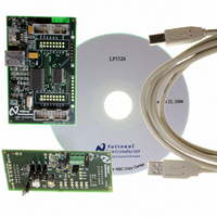
Manufacturer Part Number
LP5526TLEV
Description
BOARD EVAL LP5526 LMU LED DRIVER
Manufacturer
National Semiconductor
Series
PowerWise®r
Specifications of LP5526TLEV
Current - Output / Channel
150mA
Outputs And Type
2 (25mA), 1 (150mA)
Voltage - Output
20 V
Features
Camera Flash, Dimmable, RGB Controller
Voltage - Input
3 ~ 5.5V
Utilized Ic / Part
LP5526
Lead Free Status / RoHS Status
Not applicable / Not applicable


Power-Up Sequence
When powering up the device, V
greater than V
Magnetic Boost DC/DC Converter
The LP5526 Boost DC/DC Converter generates an 8…20V
supply voltage for the LEDs from single Li-Ion battery (3V…
4.5V). The output voltage is controlled with an 8-bit register
in 12 steps. The converter is a magnetic switching PWM mode
DC/DC converter with a current limit. Switching frequency is
1MHz, when timing resistor RT is 82kΩ. Timing resistor de-
fines the internal oscillator frequency and thus directly affects
boost frequency and RGB timings.
EMI filter (R
press EMI caused by fast switching. These components
should be as near as possible to the SW pin to ensure reliable
operation. The LP5526 Boost Converter uses pulse-skipping
elimination to stabilize the noise spectrum. Even with light
load or no load a minimum length current pulse is fed to the
inductor. An active load is used to remove the excess charge
SW
DDIO
and C
to prevent any damage to the device.
SW
) on the SW pin can be used to sup-
DD1
and V
DD2
20179776
Boost Converter Topology
should be
7
from the output capacitor at very light loads. Active load can
be disabled by writing the EN_AUTOLOAD bit low. Disabling
active load will increase slightly the efficiency at light loads,
but the downside is that pulse skipping will occur. The Boost
Converter should be stopped and set to 8V when there is no
load to minimize the current consumption.
The topology of the magnetic boost converter is called CPM
control, current programmed mode, where the inductor cur-
rent is measured and controlled with the feedback. The user
can program the output voltage of the boost converter. The
output voltage control changes the resistor divider in the feed-
back loop. The following figure shows the boost topology with
the protection circuitry. Four different protection schemes are
implemented:
1.
2.
3.
4.
Over voltage protection, limits the maximum output
voltage
— Keeps the output below breakdown voltage.
— Prevents boost operation if battery voltage is much
Over current protection, limits the maximum inductor
current
— Voltage over switching NMOS is monitored; too high
Feedback break protection. Prevents uncontrolled
operation if FB pin gets disconnected.
Duty cycle limiting, done with digital control.
higher than desired output.
voltages turn the switch off.
20179777
www.national.com
Related parts for LP5526TLEV
Image
Part Number
Description
Manufacturer
Datasheet
Request
R

Part Number:
Description:
National Semiconductor [8-Bit D/A Converter]
Manufacturer:
National Semiconductor
Datasheet:
Part Number:
Description:
National Semiconductor [Media Coprocessor]
Manufacturer:
National Semiconductor
Datasheet:
Part Number:
Description:
Digitally Controlled Tone and Volume Circuit with Stereo Audio Power Amplifier, Microphone Preamp Stage and National 3D Sound
Manufacturer:
National Semiconductor
Datasheet:
Part Number:
Description:
Digitally Controlled Tone and Volume Circuit with Stereo Audio Power Amplifier, Microphone Preamp Stage and National 3D Sound
Manufacturer:
National Semiconductor
Datasheet:
Part Number:
Description:
AC97 Rev 2 Codec with Sample Rate Conversion and National 3D Sound
Manufacturer:
National Semiconductor
Part Number:
Description:
Manufacturer:
National Semiconductor
Datasheet:
Part Number:
Description:
Manufacturer:
National Semiconductor
Datasheet:
Part Number:
Description:
General Purpose, Low Voltage, Low Power, Rail-to-Rail Output Operational Amplifiers
Manufacturer:
National Semiconductor
Datasheet:
Part Number:
Description:
8-bit 20 MSPS flash A/D converter.
Manufacturer:
National Semiconductor
Datasheet:
Part Number:
Description:
Low Noise Quad Operational Amplifier
Manufacturer:
National Semiconductor
Datasheet:
Part Number:
Description:
Quad Differential Line Receivers
Manufacturer:
National Semiconductor
Datasheet:
Part Number:
Description:
Quad High Speed Trapezoidal? Bus Transceiver
Manufacturer:
National Semiconductor
Datasheet:
Part Number:
Description:
Dual Line Receiver
Manufacturer:
National Semiconductor
Datasheet:
Part Number:
Description:
TTL to 10k ECL Level Translator with Latch
Manufacturer:
National Semiconductor
Datasheet: