LP5526TLEV National Semiconductor, LP5526TLEV Datasheet - Page 22
LP5526TLEV
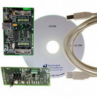
Manufacturer Part Number
LP5526TLEV
Description
BOARD EVAL LP5526 LMU LED DRIVER
Manufacturer
National Semiconductor
Series
PowerWise®r
Specifications of LP5526TLEV
Current - Output / Channel
150mA
Outputs And Type
2 (25mA), 1 (150mA)
Voltage - Output
20 V
Features
Camera Flash, Dimmable, RGB Controller
Voltage - Input
3 ~ 5.5V
Utilized Ic / Part
LP5526
Lead Free Status / RoHS Status
Not applicable / Not applicable


www.national.com
I
I
The SCL pin is used for the I
for bidirectional data transfer. Both these signals need a pull-
up resistor according to I
I
The data on SDA line must be stable during the HIGH period
of the clock signal (SCL). In other words, state of the data line
can only be changed when CLK is LOW.
I
START and STOP bits classify the beginning and the end of
the I
transitioning from HIGH to LOW while SCL line is HIGH.
STOP condition is defined as the SDA transitioning from LOW
to HIGH while SCL is HIGH. The I
START and STOP bits. The I
after START condition and free after STOP condition. During
data transmission, I
conditions. First START and repeated START conditions are
equivalent, function-wise.
w = write (SDA = “0”)
r = read (SDA = “1”)
ack = acknowledge (SDA pulled down by either master or slave)
rs = repeated start
id = 7-bit chip address, 59H (101 1001b) for LP5526.
2
2
2
2
C SIGNALS
C DATA VALIDITY
C START AND STOP CONDITIONS
C Compatible Interface
2
C session. START condition is defined as SDA signal
I
2
C Start and Stop Conditions
I
2
C Signals: Data Validity
2
C master can generate repeated START
2
C specification.
2
C clock and the SDA pin is used
2
C bus is considered to be busy
2
C master always generates
20179749
20179750
I
2
C Write Cycle
22
TRANSFERRING DATA
Every byte put on the SDA line must be eight bits long, with
the most significant bit (MSB) being transferred first. Each
byte of data has to be followed by an acknowledge bit. The
acknowledge related clock pulse is generated by the master.
The transmitter releases the SDA line (HIGH) during the ac-
knowledge clock pulse. The receiver must pull down the SDA
line during the 9
receiver which has been addressed must generate an ac-
knowledge after each byte has been received.
After the START condition, the I
dress. This address is seven bits long followed by an eighth
bit which is a data direction bit (R/W). The LP5526 address is
59H (101 1001b). For the eighth bit, a “0” indicates a WRITE
and a “1” indicates a READ. This means that the first byte is
B2H for WRITE and B3H for READ. The second byte selects
the register to which the data will be written. The third byte
contains data to write to the selected register.
Register changes take an effect at the SCL rising edge during
the last ACK from slave.
th
clock pulse, signifying an acknowledge. A
I
2
C Chip Address
2
C master sends a chip ad-
20179793
20179751
Related parts for LP5526TLEV
Image
Part Number
Description
Manufacturer
Datasheet
Request
R

Part Number:
Description:
National Semiconductor [8-Bit D/A Converter]
Manufacturer:
National Semiconductor
Datasheet:
Part Number:
Description:
National Semiconductor [Media Coprocessor]
Manufacturer:
National Semiconductor
Datasheet:
Part Number:
Description:
Digitally Controlled Tone and Volume Circuit with Stereo Audio Power Amplifier, Microphone Preamp Stage and National 3D Sound
Manufacturer:
National Semiconductor
Datasheet:
Part Number:
Description:
Digitally Controlled Tone and Volume Circuit with Stereo Audio Power Amplifier, Microphone Preamp Stage and National 3D Sound
Manufacturer:
National Semiconductor
Datasheet:
Part Number:
Description:
AC97 Rev 2 Codec with Sample Rate Conversion and National 3D Sound
Manufacturer:
National Semiconductor
Part Number:
Description:
Manufacturer:
National Semiconductor
Datasheet:
Part Number:
Description:
Manufacturer:
National Semiconductor
Datasheet:
Part Number:
Description:
General Purpose, Low Voltage, Low Power, Rail-to-Rail Output Operational Amplifiers
Manufacturer:
National Semiconductor
Datasheet:
Part Number:
Description:
8-bit 20 MSPS flash A/D converter.
Manufacturer:
National Semiconductor
Datasheet:
Part Number:
Description:
Low Noise Quad Operational Amplifier
Manufacturer:
National Semiconductor
Datasheet:
Part Number:
Description:
Quad Differential Line Receivers
Manufacturer:
National Semiconductor
Datasheet:
Part Number:
Description:
Quad High Speed Trapezoidal? Bus Transceiver
Manufacturer:
National Semiconductor
Datasheet:
Part Number:
Description:
Dual Line Receiver
Manufacturer:
National Semiconductor
Datasheet:
Part Number:
Description:
TTL to 10k ECL Level Translator with Latch
Manufacturer:
National Semiconductor
Datasheet: