LP5526TLEV National Semiconductor, LP5526TLEV Datasheet
LP5526TLEV
Specifications of LP5526TLEV


Related parts for LP5526TLEV

LP5526TLEV Summary of contents
Page 1
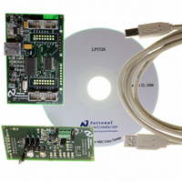
... The device is controlled through 2-wire low voltage I patible interface that reduces the number of required connec- tions. LP5526 is offered in a tiny microSMD-25 package (2. 2.54 mm). Figure 1. LP5526 Evaluation board with USB interface board © 2007 National Semiconductor Corporation National Semiconductor AN-1502 Tomi Koskela January 2007 Evaluation Kit Overview ...
Page 2
Evaluation Software LP5526 evaluation software and some support files are sup- plied on the delivery CD together with all available documen- tation regarding the circuit. You can copy the software and the files to your PC’s hard disk. The program ...
Page 3
BOOST TAB Figure 3. Boost Tab COLOR LEDS TAB Figure 4. Color LEDs Tab In this tab LP5526 boost converter can be enabled, and the output voltage can be set from the pull-down menu. The in- ternal active load can ...
Page 4
GPIO TAB Figure 5. GPIO Tab BACKLIGHT TAB Figure 6. Backlight Tab HISTORY TAB Figure 7. History Tab www.national.com In this tab it is possible to control GPIO bits and configure USB board for reading/writing. Port A, B and L ...
Page 5
Evaluation Hardware The evaluation board has the LP5526 circuit with the neces- sary external components placed around it. Test points for the circuit pins are on the board edges. PCB connectors make the connection to the USB interface board or ...
Page 6
Jumpers and Settings The following tables summarize the jumpers and proper settings. Jumper Purpose J6-J8 Shorting jumpers for current limiting resistors J17 Choose power supply V J19 Choose V DD from USB J21 Choose V DDIO interface board J25 Power ...
Page 7
USB Interface The USB interface forms the connection between the PC and the evaluation system. It converts the commands from SPI format. It also provides for adjustable supply volt- age (for the evaluation board ...
Page 8
Getting Started The following instructions show how to use the LP5526 eval- uation kit in default conditions with the USB interface board. Please use the ESD protection (ground cable) to prevent any unwanted damaging ESD events. 1. Check the jumpers ...
Page 9
Figure 10. Lp5526 Evaluation Board Schematic 9 20198209 www.national.com ...
Page 10
Board Layout Figure 11. LP5526 Evaluation board and layout picture The evaluation board layers are: 1. Top, component side 2. Signal layer 3. GND plane 4. Bottom, solder side, V DD_USB For the good performance of the circuit ...
Page 11
Fig. 12 Lp5526 Evaluation Board Layer 1 (Top, Signal). 20198210 Fig. 13 LP5526 evaluation board layer 2 (signal). 11 20198211 www.national.com ...
Page 12
Fig. 14 Lp5526 Evaluation Board Layer 3 (GND). www.national.com 20198212 Fig. 15 LP5526 evaluation board layer 4 (bottom 20198213 ). DD_USB ...
Page 13
List of Main Components Part number QTY Value, Size, Tolerance R1 1 100k 1% 0603 R2 1 150k 1% 0603 R3 27k 1% 0603 R9, R10 2 1k5 1% 0603 R14 1 82k 1% 0603 R18 1 100R ...
Page 14
... National Semiconductor and the National Semiconductor logo are registered trademarks of National Semiconductor Corporation. All other brand or product names may be trademarks or registered trademarks of their respective holders. ...