ADP1823-EVAL Analog Devices Inc, ADP1823-EVAL Datasheet - Page 26
ADP1823-EVAL
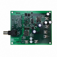
Manufacturer Part Number
ADP1823-EVAL
Description
BOARD EVAL FOR ADP1823
Manufacturer
Analog Devices Inc
Specifications of ADP1823-EVAL
Main Purpose
DC/DC, Step Down
Outputs And Type
1, Non-Isolated
Voltage - Output
1.2V
Current - Output
15A
Voltage - Input
5.5 ~ 20V
Regulator Topology
Buck
Frequency - Switching
300kHz
Board Type
Fully Populated
Utilized Ic / Part
ADP1823
Silicon Manufacturer
Analog Devices
Application Sub Type
Step Down DC/DC Converter
Kit Application Type
Power Management - Voltage Regulator
Silicon Core Number
ADP1823
Kit Contents
Board
Lead Free Status / RoHS Status
Contains lead / RoHS non-compliant
Power - Output
-
Lead Free Status / RoHS Status
Contains lead / RoHS non-compliant


•
•
•
•
ADP1823
LFCSP CONSIDERATIONS
The LFCSP has an exposed die paddle on the bottom that
efficiently conducts heat to the PCB. To achieve the optimum
performance from the LFCSP, give special consideration to the
layout of the PCB. Use the following layout guidelines for the
LFCSP:
The pad pattern is given in Figure 36. The pad dimension
should be followed closely for reliable solder joints while
maintaining reasonable clearances to prevent solder
bridging.
The thermal pad of the LFCSP provides a low thermal
impedance path to the PCB. Therefore, the PCB must be
properly designed to effectively conduct the heat away from
the package. This is achieved by adding thermal vias to the
PCB, which provide a thermal path to the inner or bottom
layers. See Figure 36 for the recommended via pattern. Note
that the via diameter is small, which prevents the solder
from flowing through the via and leaving voids in the
thermal pad solder joint.
Note that the thermal pad is attached to the die substrate;
therefore, the planes that the thermal pad is connected to
must be electrically isolated or connected to GND.
The solder mask opening should be about 120 microns
(4.7 mils) larger than the pad size, resulting in a minimum
60 microns (2.4 mils) clearance between the pad and the
solder mask.
The paste mask opening is typically designed to match the
pad size used on the peripheral pads of the LFCSP. This
technique should provide a reliable solder joint as long as
the stencil thickness is about 0.125 mm.
Rev. D | Page 26 of 32
•
•
•
•
The paste mask for the thermal pad needs to be designed for
the maximum coverage to effectively remove the heat from
the package. However, due to the presence of thermal vias
and the large size of the thermal pad, eliminating voids may
not be possible. In addition, if the solder paste coverage is
too large, solder joint defects may occur. Therefore, it is
recommended to use multiple small openings over a single
big opening in designing the paste mask. The recommended
paste mask pattern is given in Figure 36. This pattern results
in about 80% coverage, which should not degrade the
thermal performance of the package significantly.
The recommended paste mask stencil thickness is 0.125 mm.
A laser cut stainless steel stencil with trapezoidal walls
should be used.
A no-clean, Type 3 solder paste should be used for mounting
the LFCSP. In addition, a nitrogen purge during the reflow
process is recommended.
The package manufacturer recommends that the reflow
temperature should not exceed 220°C and the time above
liquid is less than 75 seconds. The preheat ramp should be
3°C per second or lower. The actual temperature profile
depends on the board density; the assembly house must
determine what works best.
Related parts for ADP1823-EVAL
Image
Part Number
Description
Manufacturer
Datasheet
Request
R

Part Number:
Description:
±1.7g Dual-Axis IMEMS Accelerometer Evaluation Board
Manufacturer:
Analog Devices Inc
Datasheet:

Part Number:
Description:
Inertial Sensor Evaluation System
Manufacturer:
Analog Devices Inc
Datasheet:
Part Number:
Description:
Manufacturer:
Analog Devices Inc
Datasheet:
Part Number:
Description:
Manufacturer:
Analog Devices Inc
Datasheet:
Part Number:
Description:
Manufacturer:
Analog Devices Inc
Datasheet:
Part Number:
Description:
Manufacturer:
Analog Devices Inc
Datasheet:
Part Number:
Description:
Manufacturer:
Analog Devices Inc
Datasheet:
Part Number:
Description:
Manufacturer:
Analog Devices Inc
Datasheet:
Part Number:
Description:
Manufacturer:
Analog Devices Inc
Datasheet:
Part Number:
Description:
Manufacturer:
Analog Devices Inc
Datasheet:
Part Number:
Description:
Manufacturer:
Analog Devices Inc
Datasheet:
Part Number:
Description:
Manufacturer:
Analog Devices Inc
Datasheet:
Part Number:
Description:
Manufacturer:
Analog Devices Inc
Datasheet: