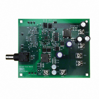
ADP1823-EVAL Analog Devices Inc, ADP1823-EVAL Datasheet - Page 14
ADP1823-EVAL
Manufacturer Part Number
ADP1823-EVAL
Description
BOARD EVAL FOR ADP1823
Manufacturer
Analog Devices Inc
Specifications of ADP1823-EVAL
Main Purpose
DC/DC, Step Down
Outputs And Type
1, Non-Isolated
Voltage - Output
1.2V
Current - Output
15A
Voltage - Input
5.5 ~ 20V
Regulator Topology
Buck
Frequency - Switching
300kHz
Board Type
Fully Populated
Utilized Ic / Part
ADP1823
Silicon Manufacturer
Analog Devices
Application Sub Type
Step Down DC/DC Converter
Kit Application Type
Power Management - Voltage Regulator
Silicon Core Number
ADP1823
Kit Contents
Board
Lead Free Status / RoHS Status
Contains lead / RoHS non-compliant
Power - Output
-
Lead Free Status / RoHS Status
Contains lead / RoHS non-compliant


ADP1823
If FREQ is driven low, the recommended SYNC input frequency
is between 600 kHz and 1.2 MHz. If FREQ is driven high, the
recommended SYNC frequency is between 1.2 MHz and
2 MHz. The FREQ setting should be carefully observed for
these SYNC frequency ranges, because the PWM voltage ramp
scales down from about 1.3 V based on the percentage of
frequency overdrive. Driving SYNC faster than recommended
for the FREQ setting results in a small ramp signal, which could
affect the signal-to-noise ratio and the modulator gain and
stability.
When an external clock is detected at the first SYNC edge, the
internal oscillator is reset and clock control shifts to SYNC.
The SYNC edges then trigger subsequent clocking of the PWM
outputs. The DH rising edges appear about 400 ns after the
corresponding SYNC edge, and the frequency is locked to the
external signal. Depending on the start-up conditions of Channel 1
and Channel 2, either Channel 1 or Channel 2 can be the first
channel synchronized to the rising edge of the SYNC clock. If
the external SYNC signal disappears during operation, the
ADP1823 reverts to its internal oscillator and experiences a
delay of no more than a single cycle of the internal oscillator.
ERROR AMPLIFIER
The ADP1823 error amplifiers are operational amplifiers. The
ADP1823 senses the output voltages through external resistor
dividers at the FB1 and FB2 pins. The FB pins are the inverting
inputs to the error amplifiers. The error amplifiers compare
these feedback voltages to the internal 0.6 V reference, and
the outputs of the error amplifiers appear at the COMP1 and
COMP2 pins. The COMP pin voltages then directly control
the duty cycle of each respective switching converter.
A series/parallel RC network is tied between the FB pins and
their respective COMP pins to provide the compensation for
the buck converter control loops. A detailed design procedure
for compensating the system is provided in the Compensating
the Voltage Mode Buck Regulator section.
The error amplifier outputs are clamped between a lower limit
of about 0.7 V and a higher limit of about 2.4 V. When the
COMP pins are low, the switching duty cycle goes to 0%, and
when the COMP pins are high, the switching duty cycle goes
to the maximum.
The SS and TRK pins are auxiliary positive inputs to the error
amplifiers. Whichever has the lowest voltage, SS, TRK, or the
internal 0.6 V reference controls the FB pin voltage and thus
the output. Therefore, if two or more of these inputs are close
to each other, a small offset is imposed on the error amplifier.
For example, if TRK approaches the 0.6 V reference, the FB
sees about 18 mV of negative offset at room temperature. For
this reason, the soft start pins have a built-in negative offset
and they charge to 0.8 V. If the TRK pins are not used, they
should be tied high to VREG.
Rev. D | Page 14 of 32
SOFT START
The ADP1823 employs a programmable soft start that reduces
input current transients and prevents output overshoot. The SS1
and SS2 pins drive auxiliary positive inputs to their respective
error amplifiers, thus the voltage at these pins regulates the voltage
at their respective feedback control pins.
Program soft start by connecting capacitors from SS1 and SS2
to GND. When starting up, the capacitor charges from an
internal 90 kΩ resistor to 0.8 V. The regulator output voltage
rises with the voltage at its respective soft start pin, allowing the
output voltage to rise slowly, reducing inrush current. See the
Soft Start section in the Applications Information section for
more information.
When a controller is disabled or experiences a current fault, the
soft start capacitor discharges through an internal 6 kΩ resistor,
so that at restart or recovery from fault, the output voltage soft
starts again.
POWER OK INDICATOR
The ADP1823 features open-drain, power OK outputs, POK1
and POK2, which sink current when their respective output
voltages drop, typically 8% below the nominal regulation
voltage. The POK pins also go low for overvoltage of typically
25%. Use this output as a logical power-good signal by connect-
ing pull-up resistors from POK1 and POK2 to VREG.
The POK1 comparator directly monitors FB1, and the threshold
is fixed at 550 mV for undervoltage and 750 mV for overvoltage.
However, the POK2 undervoltage and overvoltage comparator
input is connected to UV2 rather than FB2. For the default
thresholds at FB2, connect UV2 directly to FB2.
In a ratiometric tracking configuration, however, Channel 2 can
be configured to be a fraction of a master voltage, and thus FB2
is regulated to a voltage lower than the 0.6 V internal reference.
In this configuration, UV2 can be tied to a different tap on the
feedback divider, allowing a POK2 indication at an appropriate
output voltage threshold. See the Setting the Channel 2
Undervoltage Threshold for Ratiometric Tracking section.
TRACKING
The ADP1823 features tracking inputs, TRK1 and TRK2, which
make the output voltages track another master voltage. Voltage
tracking is especially useful in core and I/O voltage sequencing
applications where one output of the ADP1823 can be set to
track and not exceed the other, or in other multiple output
systems where specific sequencing is required.
The internal error amplifiers include three positive inputs, the
internal 0.6 V reference voltage and their respective SS and TRK
pins. The error amplifiers regulate the FB pins to the lowest of
the three inputs. To track a supply voltage, tie the TRK pin to a
resistor divider from the voltage to be tracked. See the Voltage
Tracking section.
Related parts for ADP1823-EVAL
Image
Part Number
Description
Manufacturer
Datasheet
Request
R

Part Number:
Description:
±1.7g Dual-Axis IMEMS Accelerometer Evaluation Board
Manufacturer:
Analog Devices Inc
Datasheet:

Part Number:
Description:
Inertial Sensor Evaluation System
Manufacturer:
Analog Devices Inc
Datasheet:
Part Number:
Description:
Manufacturer:
Analog Devices Inc
Datasheet:
Part Number:
Description:
Manufacturer:
Analog Devices Inc
Datasheet:
Part Number:
Description:
Manufacturer:
Analog Devices Inc
Datasheet:
Part Number:
Description:
Manufacturer:
Analog Devices Inc
Datasheet:
Part Number:
Description:
Manufacturer:
Analog Devices Inc
Datasheet:
Part Number:
Description:
Manufacturer:
Analog Devices Inc
Datasheet:
Part Number:
Description:
Manufacturer:
Analog Devices Inc
Datasheet:
Part Number:
Description:
Manufacturer:
Analog Devices Inc
Datasheet:
Part Number:
Description:
Manufacturer:
Analog Devices Inc
Datasheet:
Part Number:
Description:
Manufacturer:
Analog Devices Inc
Datasheet:
Part Number:
Description:
Manufacturer:
Analog Devices Inc
Datasheet: