ADP1823-EVAL Analog Devices Inc, ADP1823-EVAL Datasheet - Page 20
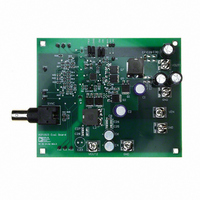
ADP1823-EVAL
Manufacturer Part Number
ADP1823-EVAL
Description
BOARD EVAL FOR ADP1823
Manufacturer
Analog Devices Inc
Specifications of ADP1823-EVAL
Main Purpose
DC/DC, Step Down
Outputs And Type
1, Non-Isolated
Voltage - Output
1.2V
Current - Output
15A
Voltage - Input
5.5 ~ 20V
Regulator Topology
Buck
Frequency - Switching
300kHz
Board Type
Fully Populated
Utilized Ic / Part
ADP1823
Silicon Manufacturer
Analog Devices
Application Sub Type
Step Down DC/DC Converter
Kit Application Type
Power Management - Voltage Regulator
Silicon Core Number
ADP1823
Kit Contents
Board
Lead Free Status / RoHS Status
Contains lead / RoHS non-compliant
Power - Output
-
Lead Free Status / RoHS Status
Contains lead / RoHS non-compliant


ADP1823
The rest of the system gain is needed to reach 0 dB at crossover.
The total gain of the system, therefore, is given by
where:
A
A
the ESR zero.
A
Additionally, the phase of the system must be brought back up
to guarantee stability. Note from the Bode plot of the filter that
the LC contributes −180° of phase shift. Additionally, because
the error amplifier is an integrator at low frequency, it contributes
an initial −90°. Therefore, before adding compensation or
accounting for the ESR zero, the system is already down −270°.
To avoid loop inversion at crossover, or −180° phase shift, a
good initial practical design is to require a phase margin of 60°,
which is therefore an overall phase loss of −120° from the initial
low frequency dc phase. The goal of the compensation is to
boost the phase back up from −270° to −120° at crossover.
Two common compensation schemes are used, which are
sometimes referred to as Type II or Type III compensation,
depending on whether the compensation design includes two
or three poles. (Dominant pole compensation, or single pole
compensation, is referred to as Type I compensation, but
unfortunately, it is not very useful for dealing successfully with
switching regulators.)
If the zero produced by the ESR of the output capacitor provides
sufficient phase boost at crossover, Type II compensation is
adequate. If the phase boost produced by the ESR of the output
capacitor is not sufficient, another zero is added to the compensa-
tion network, and thus Type III is used.
In Figure 27, the location of the ESR zero corner frequency
gives significantly different net phase at the crossover frequency.
Use the following guidelines for selecting between Type II and
Type III compensators:
If f
If f
MOD
FILTER
COMP
ESRZ
ESRZ
A
is the gain of the PWM modulator.
is the gain of the compensated error amplifier.
T
≤ f
> f
is the gain of the LC filter including the effects of
= A
CO
CO
/2, use Type II compensation.
/2, use Type III compensation.
MOD
+ A
FILTER
+ A
COMP
(26)
Rev. D | Page 20 of 32
The following equations were used for the calculation of the
compensation components as shown in Figure 28 and Figure 29:
where:
f
f
f
f
PHASE
Z1
Z2
P1
P2
GAIN
is the zero produced in the Type II compensation.
is the zero produced in the Type III compensation.
is the pole produced in the Type II compensation.
in the pole produced in the Type III compensation.
f
f
f
f
Z
Z
P
P
0dB
0°
–90°
–180°
1
1
2
2
=
=
=
=
PHASE CONTRIBUTION AT CROSSOVER
π 2
π 2
–40dB/dec
–20dB/dec
π 2
π 2
OF VARIOUS ESR ZERO CORNERS
R
R
C
R
1
Z
Z
FF
FF
1
LC FILTER BODE PLOT
C
f
C
LC
C
I
(
1
C
R
I
FF
f
Figure 27. LC Filter Bode Plot
1
TOP
I
ESR1
+
C
C
HF
HF
+
f
ESR2
R
FF
f
ESR3
)
f
CO
Φ
Φ
Φ
1
2
3
f
SW
FREQUENCY
(27)
(28)
(29)
(30)
Related parts for ADP1823-EVAL
Image
Part Number
Description
Manufacturer
Datasheet
Request
R

Part Number:
Description:
±1.7g Dual-Axis IMEMS Accelerometer Evaluation Board
Manufacturer:
Analog Devices Inc
Datasheet:

Part Number:
Description:
Inertial Sensor Evaluation System
Manufacturer:
Analog Devices Inc
Datasheet:
Part Number:
Description:
Manufacturer:
Analog Devices Inc
Datasheet:
Part Number:
Description:
Manufacturer:
Analog Devices Inc
Datasheet:
Part Number:
Description:
Manufacturer:
Analog Devices Inc
Datasheet:
Part Number:
Description:
Manufacturer:
Analog Devices Inc
Datasheet:
Part Number:
Description:
Manufacturer:
Analog Devices Inc
Datasheet:
Part Number:
Description:
Manufacturer:
Analog Devices Inc
Datasheet:
Part Number:
Description:
Manufacturer:
Analog Devices Inc
Datasheet:
Part Number:
Description:
Manufacturer:
Analog Devices Inc
Datasheet:
Part Number:
Description:
Manufacturer:
Analog Devices Inc
Datasheet:
Part Number:
Description:
Manufacturer:
Analog Devices Inc
Datasheet:
Part Number:
Description:
Manufacturer:
Analog Devices Inc
Datasheet: