ADP1823-EVAL Analog Devices Inc, ADP1823-EVAL Datasheet - Page 19
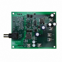
ADP1823-EVAL
Manufacturer Part Number
ADP1823-EVAL
Description
BOARD EVAL FOR ADP1823
Manufacturer
Analog Devices Inc
Specifications of ADP1823-EVAL
Main Purpose
DC/DC, Step Down
Outputs And Type
1, Non-Isolated
Voltage - Output
1.2V
Current - Output
15A
Voltage - Input
5.5 ~ 20V
Regulator Topology
Buck
Frequency - Switching
300kHz
Board Type
Fully Populated
Utilized Ic / Part
ADP1823
Silicon Manufacturer
Analog Devices
Application Sub Type
Step Down DC/DC Converter
Kit Application Type
Power Management - Voltage Regulator
Silicon Core Number
ADP1823
Kit Contents
Board
Lead Free Status / RoHS Status
Contains lead / RoHS non-compliant
Power - Output
-
Lead Free Status / RoHS Status
Contains lead / RoHS non-compliant


COMPENSATING THE VOLTAGE MODE BUCK
REGULATOR
Assuming the LC filter design is complete, the feedback control
system can then be compensated. Good compensation is critical
to proper operation of the regulator. Calculate the quantities in
Equation 19 through Equation 47 to derive the compensation
values. The goal is to guarantee that the voltage gain of the buck
converter crosses unity at a slope that provides adequate phase
margin for stable operation. Additionally, at frequencies above
the crossover frequency, f
and attenuation of switching noise are important secondary
goals. For initial practical designs, a good choice for the
crossover frequency is one tenth of the switching frequency.
First calculate
This gives sufficient frequency range to design a compensation
that attenuates switching artifacts, while also giving sufficient
control loop bandwidth to provide good transient response.
The output LC filter is a resonant network that inflicts two poles
upon the response at a frequency f
Generally, the LC corner frequency is about two orders of
magnitude below the switching frequency, and, therefore, about
one order of magnitude below crossover. To achieve sufficient
phase margin at crossover to guarantee stability, the design
must compensate for the two poles at the LC corner frequency
with two zeros to boost the system phase prior to crossover. The
two zeros require an additional pole or two above the crossover
frequency to guarantee adequate gain margin and attenuation of
switching noise at high frequencies.
Depending on component selection, one zero may already be
generated by the equivalent series resistance (ESR) of the output
capacitor. Calculate this zero corner frequency, f
Figure 26 shows a typical Bode plot of the LC filter by itself.
The gain of the LC filter at crossover can be linearly
approximated from Figure 26 as
If f
between the exact solution and the linear approximation.
ESR
A
A
≈ f
f
f
f
CO
LC
ESR
FILTER
FILTER
CO
=
=
=
, add another 3 dB to account for the local difference
2
= A
f
2
10
π
SW
=
π
1
−
R
LC
LC
40
ESR
+ A
1
dB
C
OUT
ESR
×
CO
log
, guaranteeing sufficient gain margin
⎛
⎜
⎜
⎝
f
f
ESR
LC
⎞
⎟
⎟
⎠
LC
−
, so next calculate
20
dB
×
log
ESR
⎛
⎜
⎜
⎝
, as
f
f
ESR
CO
⎞
⎟
⎟
⎠
(19)
(20)
(21)
(22)
Rev. D | Page 19 of 32
To compensate the control loop, the gain of the system must be
brought back up so that it is 0 dB at the desired crossover
frequency. Some gain is provided by the PWM modulation itself.
For systems using the internal oscillator, this becomes
Note that if the converter is being synchronized, the ramp
voltage, V
frequency increase over the nominal setting of the FREQ pin.
The factor of 2 in the numerator takes into account that the
SYNC frequency is divided by 2 to generate the switching
frequency. For example, if the FREQ pin is set high for the
600 kHz range and a 2 MHz SYNC signal is applied, the ramp
voltage is 0.78 V. The gain of the modulator is increased by
4.4 dB in this example.
PHASE
GAIN
V
A
A
RAMP
MOD
MOD
0dB
0°
–90°
–180°
RAMP
=
=
=
–40dB/dec
20
, is lower than 1.3 V by the percentage of
20
1
3 .
LC FILTER BODE PLOT
log
log
V
f
⎛
⎜
⎜
⎝
LC
Figure 26. LC Filter Bode Plot
⎛
⎜
⎜
⎝
1
⎛
⎜
⎜
⎝
–20dB/dec
V
V
3 .
2
V
IN
RAMP
f
V
SYNC
f
IN
f
ESR
FREQ
⎞
⎟
⎟
⎠
⎞
⎟
⎟
⎠
⎞
⎟
⎟
⎠
f
CO
Φ
A
FILTER
FILTER
f
SW
ADP1823
FREQUENCY
(23)
(24)
(25)
Related parts for ADP1823-EVAL
Image
Part Number
Description
Manufacturer
Datasheet
Request
R

Part Number:
Description:
±1.7g Dual-Axis IMEMS Accelerometer Evaluation Board
Manufacturer:
Analog Devices Inc
Datasheet:

Part Number:
Description:
Inertial Sensor Evaluation System
Manufacturer:
Analog Devices Inc
Datasheet:
Part Number:
Description:
Manufacturer:
Analog Devices Inc
Datasheet:
Part Number:
Description:
Manufacturer:
Analog Devices Inc
Datasheet:
Part Number:
Description:
Manufacturer:
Analog Devices Inc
Datasheet:
Part Number:
Description:
Manufacturer:
Analog Devices Inc
Datasheet:
Part Number:
Description:
Manufacturer:
Analog Devices Inc
Datasheet:
Part Number:
Description:
Manufacturer:
Analog Devices Inc
Datasheet:
Part Number:
Description:
Manufacturer:
Analog Devices Inc
Datasheet:
Part Number:
Description:
Manufacturer:
Analog Devices Inc
Datasheet:
Part Number:
Description:
Manufacturer:
Analog Devices Inc
Datasheet:
Part Number:
Description:
Manufacturer:
Analog Devices Inc
Datasheet:
Part Number:
Description:
Manufacturer:
Analog Devices Inc
Datasheet: