ADP1823-EVAL Analog Devices Inc, ADP1823-EVAL Datasheet - Page 25
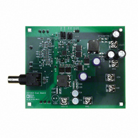
ADP1823-EVAL
Manufacturer Part Number
ADP1823-EVAL
Description
BOARD EVAL FOR ADP1823
Manufacturer
Analog Devices Inc
Specifications of ADP1823-EVAL
Main Purpose
DC/DC, Step Down
Outputs And Type
1, Non-Isolated
Voltage - Output
1.2V
Current - Output
15A
Voltage - Input
5.5 ~ 20V
Regulator Topology
Buck
Frequency - Switching
300kHz
Board Type
Fully Populated
Utilized Ic / Part
ADP1823
Silicon Manufacturer
Analog Devices
Application Sub Type
Step Down DC/DC Converter
Kit Application Type
Power Management - Voltage Regulator
Silicon Core Number
ADP1823
Kit Contents
Board
Lead Free Status / RoHS Status
Contains lead / RoHS non-compliant
Power - Output
-
Lead Free Status / RoHS Status
Contains lead / RoHS non-compliant


PCB LAYOUT GUIDELINES
In any switching converter, some circuit paths carry high dI/dt,
which can create spikes and noise. Other circuit paths are
sensitive to noise. Still others carry high dc current and can
produce significant IR voltage drops. The key to proper PCB
layout of a switching converter is to identify these critical paths
and arrange the components and copper area accordingly.
When designing PCB layouts, be sure to keep high current
loops small. In addition, keep compensation and feedback
components away from the switch nodes and their associated
components.
The following is a list of recommended layout practices for the
ADP1823, arranged by decreasing order of importance.
• The current waveform in the top and bottom FETs is a pulse
• GND, the VREG bypass, the soft start capacitor, and the
• The PGND pin handles high dI/dt gate drive current
with very high dI/dt; therefore, the path to, through, and from
each individual FET should be as short as possible and the
two paths should be commoned as much as possible. In
designs that use a pair of D-Pak or SO-8 FETs on one side
of the PCB, it is best to counter-rotate the two so that the
switch node is on one side of the pair and the high-side
drain can be bypassed to the low-side source with a suitable
ceramic bypass capacitor, placed as close as possible to the
FETs to minimize inductance around this loop through the
FETs and capacitor. The recommended bypass ceramic
capacitor values range from 1 μF to 22 μF depending upon
the output current. This bypass capacitor is usually connected
to a larger value bulk filter capacitor and should be grounded to
the PGND plane.
bottom end of the output feedback divider resistors should
be tied to an (almost isolated) small AGND plane. All of
these connections should have connections from the pin
to the AGND plane that are as short as possible. No high
current or high dI/dt signals should be connected to
this AGND plane. The AGND area should be connected
through one wide trace to the negative terminal of the
output filter capacitors.
returning from the source of the low-side MOSFET. The
voltage at this pin also establishes the 0 V reference for the
overcurrent limit protection (OCP) function and the CSL
pin. A small PGND plane should connect the PGND pin
and the PVCC bypass capacitor through a wide and direct
path to the source of the low-side MOSFET. The placement
of C
terminal of C
the low-side MOSFET.
IN
is critical for controlling ground bounce. The negative
IN
needs to be placed very close to the source of
Rev. D | Page 25 of 32
• Avoid long traces or large copper areas at the FB and CSL
• The switch node is the noisiest place in the switcher circuit
• Gate drive traces (DH and DL) handle high dI/dt and,
• The negative terminal of output filter capacitors should be
• Generally, be sure that all traces are sized according to the
pins, which are low signal level inputs that are sensitive to
capacitive and inductive noise pickup. It is best to position
any series resistors and capacitors as close as possible to
these pins. Avoid running these traces close and parallel to
high dI/dt traces.
with large ac and dc voltage and current. This node should
be wide to minimize resistive voltage drop. However, to
minimize the generation of capacitively coupled noise, the
total area should be small. Place the FETs and inductor all
close together on a small copper plane to minimize series
resistance and keep the copper area small.
therefore, they tend to produce noise and ringing. They
should be as short and direct as possible. If possible, avoid
using feedthrough vias in the gate drive traces. If vias are
needed, it is best to use two relatively large ones in parallel
to reduce the peak current density and the current in each
via. If the overall PCB layout is less than optimal, slowing
down the gate drive slightly can be very helpful to reduce
noise and ringing. It is occasionally helpful to place small
value resistors (such as 5 Ω or 10 Ω) in series with the gate
leads, mainly DH traces to the high-side FET gates. These
can be populated with 0 Ω resistors if resistance is not
needed. Note that the added gate resistance increases the
switching rise and fall times and that in turn increases the
switching power loss in the MOSFET.
tied closely to the source of the low-side FET. Doing this
helps to minimize voltage difference between GND and
PGND at the ADP1823.
current to be handled as well as their sensitivity in the
circuit. Standard PCB layout guidelines mainly address
heating effects of current in a copper conductor. These are
completely valid, but they do not fully cover other concerns,
such as stray inductance or dc voltage drop. Any dc voltage
differential in connections between ADP1823 GND and the
converter power output ground can cause a significant
output voltage error, because it affects converter output
voltage according to the ratio with the 600 mV feedback
reference. For example, a 6 mV offset between ground on the
ADP1823 and the converter power output causes a 1% error
in the converter output voltage.
ADP1823
Related parts for ADP1823-EVAL
Image
Part Number
Description
Manufacturer
Datasheet
Request
R

Part Number:
Description:
±1.7g Dual-Axis IMEMS Accelerometer Evaluation Board
Manufacturer:
Analog Devices Inc
Datasheet:

Part Number:
Description:
Inertial Sensor Evaluation System
Manufacturer:
Analog Devices Inc
Datasheet:
Part Number:
Description:
Manufacturer:
Analog Devices Inc
Datasheet:
Part Number:
Description:
Manufacturer:
Analog Devices Inc
Datasheet:
Part Number:
Description:
Manufacturer:
Analog Devices Inc
Datasheet:
Part Number:
Description:
Manufacturer:
Analog Devices Inc
Datasheet:
Part Number:
Description:
Manufacturer:
Analog Devices Inc
Datasheet:
Part Number:
Description:
Manufacturer:
Analog Devices Inc
Datasheet:
Part Number:
Description:
Manufacturer:
Analog Devices Inc
Datasheet:
Part Number:
Description:
Manufacturer:
Analog Devices Inc
Datasheet:
Part Number:
Description:
Manufacturer:
Analog Devices Inc
Datasheet:
Part Number:
Description:
Manufacturer:
Analog Devices Inc
Datasheet:
Part Number:
Description:
Manufacturer:
Analog Devices Inc
Datasheet: