ADP1823-EVAL Analog Devices Inc, ADP1823-EVAL Datasheet - Page 24
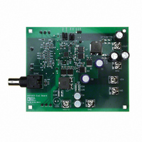
ADP1823-EVAL
Manufacturer Part Number
ADP1823-EVAL
Description
BOARD EVAL FOR ADP1823
Manufacturer
Analog Devices Inc
Specifications of ADP1823-EVAL
Main Purpose
DC/DC, Step Down
Outputs And Type
1, Non-Isolated
Voltage - Output
1.2V
Current - Output
15A
Voltage - Input
5.5 ~ 20V
Regulator Topology
Buck
Frequency - Switching
300kHz
Board Type
Fully Populated
Utilized Ic / Part
ADP1823
Silicon Manufacturer
Analog Devices
Application Sub Type
Step Down DC/DC Converter
Kit Application Type
Power Management - Voltage Regulator
Silicon Core Number
ADP1823
Kit Contents
Board
Lead Free Status / RoHS Status
Contains lead / RoHS non-compliant
Power - Output
-
Lead Free Status / RoHS Status
Contains lead / RoHS non-compliant


ADP1823
Setting the Channel 2 Undervoltage Threshold for
Ratiometric Tracking
If FB2 is regulated to a voltage lower than 0.6 V by configuring
TRK2 for ratiometric tracking, the Channel 2 undervoltage
threshold can be set appropriately by splitting the top resistor
in the voltage divider, as shown in Figure 33. R
calculated for the compensation in Equation 52, and
The current in all the resistors is the same.
where:
V
V
tracking calculations.
V
Solving for R
UV2
FB2
OUT2
is the feedback voltage value set during the ratiometric
R
is 600 mV.
POK2
R
R
R
V
is the Channel 2 output voltage.
TOP
A
B
BOT
FB
Figure 33. Setting the Channel 2 Undervoltage Threshold
=
=
2
= R
R
R
=
BOT
BOT
A
A
V
+ R
and R
UV
TO ERROR
AMPLIFIER
(
(
V
V
2
B
UV
OUTA
R
B
−
B
V
B
2
V
,
B
V
FB
−
2
FB
FB
2
V
−
2
2
FB
V
=
2
UV
)
V
2
)
OUT
2
R
−
550mV
750mV
A
V
UV
2
UV2
FB2
BOT
CHANNEL 2
VOLTAGE
OUTPUT
is the same as
R
R
R
A
B
BOT
(53)
(54)
(55)
(56)
Rev. D | Page 24 of 32
THERMAL CONSIDERATIONS
The current required to drive the external MOSFETs comprises
the vast majority of the power dissipation of the ADP1823. The
on-chip LDO regulates down to 5 V, and this 5 V supplies the
drivers. The full gate drive current passes through the LDO and
is then dissipated in the gate drivers. The power dissipated on
the gate drivers on the ADP1823 is
where:
V
f
Q numbers are the total gate charge specifications from the
selected MOSFET data sheets.
The power dissipation heats the ADP1823. As the switching
frequency, the input voltage, and the MOSFET size increase, the
power dissipation on the ADP1823 increases. Care must be taken
not to exceed the maximum junction temperature. To calculate
the junction temperature from the ambient temperature and
power dissipation
The thermal resistance, θ
depending on board layout, and the maximum specified junction
temperature is 125°C, which means that at a maximum ambient
temperature of 85°C without airflow, the maximum dissipation
allowed is about 1 W.
A thermal shutdown protection circuit on the ADP1823 shuts
off the LDO and the controllers if the die temperature exceeds
approximately 145°C, but this is a gross fault protection only
and should not be relied upon for system reliability.
SW
IN
is the switching frequency.
is the voltage applied to IN.
P
T
D
J
= T
= V
A
IN
+ P
f
SW
D
(Q
θ
DH1
JA
+ Q
JA
DL1
, of the package is typically 40°C/W
+ Q
DH2
+ Q
DL2
)
(57)
(58)
Related parts for ADP1823-EVAL
Image
Part Number
Description
Manufacturer
Datasheet
Request
R

Part Number:
Description:
±1.7g Dual-Axis IMEMS Accelerometer Evaluation Board
Manufacturer:
Analog Devices Inc
Datasheet:

Part Number:
Description:
Inertial Sensor Evaluation System
Manufacturer:
Analog Devices Inc
Datasheet:
Part Number:
Description:
Manufacturer:
Analog Devices Inc
Datasheet:
Part Number:
Description:
Manufacturer:
Analog Devices Inc
Datasheet:
Part Number:
Description:
Manufacturer:
Analog Devices Inc
Datasheet:
Part Number:
Description:
Manufacturer:
Analog Devices Inc
Datasheet:
Part Number:
Description:
Manufacturer:
Analog Devices Inc
Datasheet:
Part Number:
Description:
Manufacturer:
Analog Devices Inc
Datasheet:
Part Number:
Description:
Manufacturer:
Analog Devices Inc
Datasheet:
Part Number:
Description:
Manufacturer:
Analog Devices Inc
Datasheet:
Part Number:
Description:
Manufacturer:
Analog Devices Inc
Datasheet:
Part Number:
Description:
Manufacturer:
Analog Devices Inc
Datasheet:
Part Number:
Description:
Manufacturer:
Analog Devices Inc
Datasheet: