ADP1823-EVAL Analog Devices Inc, ADP1823-EVAL Datasheet - Page 17
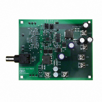
ADP1823-EVAL
Manufacturer Part Number
ADP1823-EVAL
Description
BOARD EVAL FOR ADP1823
Manufacturer
Analog Devices Inc
Specifications of ADP1823-EVAL
Main Purpose
DC/DC, Step Down
Outputs And Type
1, Non-Isolated
Voltage - Output
1.2V
Current - Output
15A
Voltage - Input
5.5 ~ 20V
Regulator Topology
Buck
Frequency - Switching
300kHz
Board Type
Fully Populated
Utilized Ic / Part
ADP1823
Silicon Manufacturer
Analog Devices
Application Sub Type
Step Down DC/DC Converter
Kit Application Type
Power Management - Voltage Regulator
Silicon Core Number
ADP1823
Kit Contents
Board
Lead Free Status / RoHS Status
Contains lead / RoHS non-compliant
Power - Output
-
Lead Free Status / RoHS Status
Contains lead / RoHS non-compliant


In the case of output capacitors where the impedance of the
ESR and ESL are small at the switching frequency, for instance,
where the output capacitor is a bank of parallel MLCC
capacitors, the capacitive impedance dominates and the ripple
equation reduces to
Make sure that the ripple current rating of the output capacitors
is greater than the maximum inductor ripple current.
During a load step transient on the output, the output capacitor
supplies the load until the control loop has a chance to ramp the
inductor current. This initial output voltage deviation due to a
change in load is dependent on the output capacitor characteristics.
Again, usually the capacitor ESR dominates this response, and
the ΔV
value for ΔI
SELECTING THE MOSFETs
The choice of MOSFET directly affects the dc-to-dc converter
performance. The MOSFET must have low on resistance (R
to reduce I
In addition, the MOSFET must have low thermal resistance to
ensure that the power dissipated in the MOSFET does not result
in overheating.
The power switch, or high-side MOSFET, carries the load current
during the PWM on time, carries the transition loss of the
switching behavior, and requires gate charge drive to switch.
Typically, the smaller the MOSFET R
charge and vice versa. Therefore, it is important to choose a
high-side MOSFET that balances those two losses. The conduction
loss of the high-side MOSFET is determined by
where:
P
R
The gate charge losses are dissipated by the ADP1823 regulator
and gate drivers and affect the efficiency of the system. The gate
charge loss is approximated by
where:
P
Q
f
Making the conduction losses balance the gate charge losses
usually yields the most efficient choice.
SW
C
DSON
G
G
is the conduction power loss.
is the gate charge power.
is the MOSFET total gate charge.
is the converter switching frequency.
Δ
P
P ≅
is the MOSFET on resistance.
C
G
V
OUT
OUT
≅
2
in Equation 6 can be used with the load step current
V
R losses and low gate charge to reduce switching losses.
I
L
L
≅
.
IN
2
R
8
Q
DSON
C
G
OUT
f
Δ
SW
I
V
L
V
OUT
f
IN
SW
DSON
, the higher the gate
DSON
Rev. D | Page 17 of 32
)
(7)
(8)
(9)
Furthermore, the high-side MOSFET transition loss is
approximated by
where t
MOSFET as stated in the MOSFET data sheet.
The total power dissipation of the high-side MOSFET is
the sum of the previous losses.
where P
dissipation heats the high-side MOSFET.
The conduction losses may need an adjustment to account
for the MOSFET R
MOSFET R
MOSFET data sheet should list the thermal resistance of the
package, θ
coefficient of R
calculate the MOSFET junction temperature rise over the
ambient temperature of interest.
Next, calculate the new R
curve and the R
temperature coefficient (TC) of R
alternate method to calculate the MOSFET R
temperature, T
Then the conduction losses can be recalculated and the procedure
iterated once or twice until the junction temperature calculations
are relatively consistent.
The synchronous rectifier, or low-side MOSFET, carries the
inductor current when the high-side MOSFET is off. For high
input voltage and low output voltage, the low-side MOSFET
carries the current most of the time, and therefore, to achieve
high efficiency it is critical to optimize the low-side MOSFET
for small on resistance. In cases where the power loss exceeds
the MOSFET rating, or lower resistance is required than is
available in a single MOSFET, connect multiple low-side
MOSFETs in parallel. The equation for low-side MOSFET
power loss is
where:
P
R
side MOSFETs.
Check the gate charge losses of the synchronous rectifier(s)
using the P
reasonable.
LS
DSON
is the low-side MOSFET on resistance.
P
T
R
P
P
is the parallel combination of the resistances of the low-
D
J
DSON
T
LS
= T
R
= P
D
≅
and t
≅
is the total high-side MOSFET power loss. This
JA
@ T
A
V
C
G
DSON
, along with a normalized curve of the temperature
I
+ θ
+ P
L
equation (Equation 9) to make sure they are
IN
2
F
J
R
I
DSON
J
are the rise and fall times of the selected
DSON
, is
JA
= R
L
G
DSON
increases with increasing temperature. The
(
t
+ P
P
R
DSON
D
. For the power dissipation estimated,
specification at 25°C. A typical value of the
DSON
2
+
⎛
⎜
⎜
⎝
T
1
t
variation with temperature. Note that
@ 25°C[1 + TC ( T
F
−
)
DSON
V
f
V
SW
OUT
IN
from the temperature coefficient
⎞
⎟
⎟
⎠
DSON
is 0.004/°C; therefore, an
J
− 25°C)]
DSON
at a second
ADP1823
(10)
(11)
(12)
(14)
(13)
Related parts for ADP1823-EVAL
Image
Part Number
Description
Manufacturer
Datasheet
Request
R

Part Number:
Description:
±1.7g Dual-Axis IMEMS Accelerometer Evaluation Board
Manufacturer:
Analog Devices Inc
Datasheet:

Part Number:
Description:
Inertial Sensor Evaluation System
Manufacturer:
Analog Devices Inc
Datasheet:
Part Number:
Description:
Manufacturer:
Analog Devices Inc
Datasheet:
Part Number:
Description:
Manufacturer:
Analog Devices Inc
Datasheet:
Part Number:
Description:
Manufacturer:
Analog Devices Inc
Datasheet:
Part Number:
Description:
Manufacturer:
Analog Devices Inc
Datasheet:
Part Number:
Description:
Manufacturer:
Analog Devices Inc
Datasheet:
Part Number:
Description:
Manufacturer:
Analog Devices Inc
Datasheet:
Part Number:
Description:
Manufacturer:
Analog Devices Inc
Datasheet:
Part Number:
Description:
Manufacturer:
Analog Devices Inc
Datasheet:
Part Number:
Description:
Manufacturer:
Analog Devices Inc
Datasheet:
Part Number:
Description:
Manufacturer:
Analog Devices Inc
Datasheet:
Part Number:
Description:
Manufacturer:
Analog Devices Inc
Datasheet: