NCP1605FORWGEVB ON Semiconductor, NCP1605FORWGEVB Datasheet - Page 30
NCP1605FORWGEVB
Manufacturer Part Number
NCP1605FORWGEVB
Description
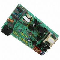
EVAL BOARD FOR NCP1605FORWG
Manufacturer
ON Semiconductor
Datasheets
1.NCP1217P100G.pdf
(19 pages)
2.NCP1605ADR2G.pdf
(32 pages)
3.NCP1605FORWGEVB.pdf
(2 pages)
4.NCP1605FORWGEVB.pdf
(20 pages)
Specifications of NCP1605FORWGEVB
Design Resources
NCP1605FORWGEVB BOM NCP1605FORWGEVB Gerber Files NCP1605 EVB Schematic
Main Purpose
AC/DC, Primary and Secondary Side with PFC
Outputs And Type
1, Isolated
Voltage - Output
19V
Current - Output
8A
Voltage - Input
90 ~ 265VAC
Regulator Topology
Forward Converter
Frequency - Switching
133kHz
Board Type
Fully Populated
Utilized Ic / Part
NCP1217, NCP1605
Lead Free Status / RoHS Status
Lead free / RoHS Compliant
Power - Output
-
Lead Free Status / Rohs Status
Lead free / RoHS Compliant
For Use With/related Products
NCP1605FORWG
Other names
NCP1605FORWGEVBOS


Fault Management Block
(“BO_NOK”),
(“STDWN”), Die Overtemperature (“TSD”), the circuit
immediately turns off and recovers operation as soon as the
fault disappears.
circuit keeps off until the end of the next V
by the HV startup current source.
When any of the following faults is detected: brown−out
In case of UVLO (V
The following block diagram details the function.
V
V
Brown−Out
Pin Voltage
Drive Output
Circuit State
pfcOK
CC
OUT
When the high voltage, startup current source is on, the brown−out is active and its threshold is the upper one (V
Undervoltage
CC
V
OFF
CC
too low to allow operation), the
ON
1 V
(“UVP”),
Figure 71. Startup and Brown Out Conditions
CC
charge phase
shutdown
The Circuit is Off ≥ Low Consumption
http://onsemi.com
30
(Vcc<VccOFF)
V
1 V
CC
UVLO
OFF
Figure 72. Fault Management Block
TSD
Shutdown
Thermal
Internal
HVCS_ON
V
S
out
R
UVLO
Latch
Stdwn
Regulation Level
UVP
Q
V
CC
0.5 V
STUP
BO
= V
BO
H = 1 V).
BO_NOK
OFF
Related parts for NCP1605FORWGEVB
Image
Part Number
Description
Manufacturer
Datasheet
Request
R

Part Number:
Description:
ON Semiconductor [VOLTAGE REGULATOR]
Manufacturer:
ON Semiconductor
Datasheet:
Part Number:
Description:
357-036-542-201 CARDEDGE 36POS DL .156 BLK LOPRO
Manufacturer:
ON Semiconductor
Datasheet:
Part Number:
Description:
357-036-542-201 CARDEDGE 36POS DL .156 BLK LOPRO
Manufacturer:
ON Semiconductor
Datasheet:
Part Number:
Description:
357-036-542-201 CARDEDGE 36POS DL .156 BLK LOPRO
Manufacturer:
ON Semiconductor
Datasheet:
Part Number:
Description:
357-036-542-201 CARDEDGE 36POS DL .156 BLK LOPRO
Manufacturer:
ON Semiconductor
Datasheet:
Part Number:
Description:
357-036-542-201 CARDEDGE 36POS DL .156 BLK LOPRO
Manufacturer:
ON Semiconductor
Datasheet:
Part Number:
Description:
357-036-542-201 CARDEDGE 36POS DL .156 BLK LOPRO
Manufacturer:
ON Semiconductor
Datasheet:
Part Number:
Description:
357-036-542-201 CARDEDGE 36POS DL .156 BLK LOPRO
Manufacturer:
ON Semiconductor
Datasheet:
Part Number:
Description:
357-036-542-201 CARDEDGE 36POS DL .156 BLK LOPRO
Manufacturer:
ON Semiconductor
Datasheet:
Part Number:
Description:
357-036-542-201 CARDEDGE 36POS DL .156 BLK LOPRO
Manufacturer:
ON Semiconductor
Datasheet:
Part Number:
Description:
357-036-542-201 CARDEDGE 36POS DL .156 BLK LOPRO
Manufacturer:
ON Semiconductor
Datasheet:
Part Number:
Description:
Manufacturer:
ON Semiconductor
Datasheet:
Part Number:
Description:
Manufacturer:
ON Semiconductor
Datasheet:
Part Number:
Description:
Manufacturer:
ON Semiconductor
Datasheet: