NCP1605FORWGEVB ON Semiconductor, NCP1605FORWGEVB Datasheet - Page 20
NCP1605FORWGEVB
Manufacturer Part Number
NCP1605FORWGEVB
Description
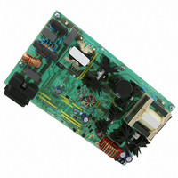
EVAL BOARD FOR NCP1605FORWG
Manufacturer
ON Semiconductor
Datasheets
1.NCP1217P100G.pdf
(19 pages)
2.NCP1605ADR2G.pdf
(32 pages)
3.NCP1605FORWGEVB.pdf
(2 pages)
4.NCP1605FORWGEVB.pdf
(20 pages)
Specifications of NCP1605FORWGEVB
Design Resources
NCP1605FORWGEVB BOM NCP1605FORWGEVB Gerber Files NCP1605 EVB Schematic
Main Purpose
AC/DC, Primary and Secondary Side with PFC
Outputs And Type
1, Isolated
Voltage - Output
19V
Current - Output
8A
Voltage - Input
90 ~ 265VAC
Regulator Topology
Forward Converter
Frequency - Switching
133kHz
Board Type
Fully Populated
Utilized Ic / Part
NCP1217, NCP1605
Lead Free Status / RoHS Status
Lead free / RoHS Compliant
Power - Output
-
Lead Free Status / Rohs Status
Lead free / RoHS Compliant
For Use With/related Products
NCP1605FORWG
Other names
NCP1605FORWGEVBOS


Regulation Block and Low Output Voltage Detection
inverting input and output is provided. It features a typical
transconductance gain of 200 mS and a maximum
capability of ±20 mA. The output voltage of the PFC stage
is typically scaled down by a resistors divider and
monitored by the inverting input (feedback pin − Pin 4).
The bias current is minimized (less than 500 nA) to allow
the use of a high impedance feedback network. The output
of the error amplifier is pinned out for external loop
compensation (Pin 3). Typically a capacitor in the range of
100 nF, is applied between Pin 3 and ground, to set the
regulation bandwidth below 20 Hz, as need in PFC
applications.
variations of the load, may result in excessive over and
undershoots. Overshoots are limited by the Overvoltage
Protection (see OVP section). To contain the undershoots, an
internal comparator monitors the feedback (V
V
V
Figure 57. Input Voltage and On−time vs Time (example with F
control
Pin4
A transconductance error amplifier with access to the
Provided the low bandwidth of the regulation loop, sharp
350,00
300,00
250,00
200,00
150,00
100,00
FB
50,00
0,00
is lower than 95.5% of its nominal value, it connects a
0
0.955*Vref
Figure 58. Regulation Block
OFF
OVLflag1
V
ref
V
2
Detect
out
Low
+
+
-
-
3 V
Amplifier
Error
4
pfcOK
±20 mA
+
2R
V
R
F
V
REGUL
6
Pin4
200 mA
) and when
http://onsemi.com
8
+
V
F
time (ms)
20
10
an accurate range:
•
•
offset down by (V
to the “V
Finally, the output of the regulation is a signal (“V
of the block diagram) that varies between 0 and 1 V.
200 mA current source to speed−up the charge of the
compensation capacitor (Cpin3). Finally, it is like if the
comparator multiplied the error amplifier gain by 10.
is not enabled during the startup sequence of the PFC stage
but only once the converter has stabilized (that is when the
V
The swing of the error amplifier output is limited within
Hence, V
One must note that this circuitry for undershoots limitation,
It is forced above a voltage drop (V
It is clamped not to exceed 3.0 V + the same V
drop.
REGUL
SW
= 100 kHz, Pin =150 W, V
Figure 59. Correspondence between V
12
TON
0 V
Pin3
processing block” and the PWM section.
V
features a 3 V voltage swing. V
F
F
1 V
) and divided by three before it connects
14
and V
16
REGUL
AC
3 V + V
= 230 V, L = 200 mH)
F
) by some circuitry.
18
F
V
CONTROL
Pin3
CONTROL
F
voltage
REGUL
20
is then
3,50
3,00
2,50
2,00
1,50
1,00
0,50
0,00
”
Related parts for NCP1605FORWGEVB
Image
Part Number
Description
Manufacturer
Datasheet
Request
R

Part Number:
Description:
ON Semiconductor [VOLTAGE REGULATOR]
Manufacturer:
ON Semiconductor
Datasheet:
Part Number:
Description:
357-036-542-201 CARDEDGE 36POS DL .156 BLK LOPRO
Manufacturer:
ON Semiconductor
Datasheet:
Part Number:
Description:
357-036-542-201 CARDEDGE 36POS DL .156 BLK LOPRO
Manufacturer:
ON Semiconductor
Datasheet:
Part Number:
Description:
357-036-542-201 CARDEDGE 36POS DL .156 BLK LOPRO
Manufacturer:
ON Semiconductor
Datasheet:
Part Number:
Description:
357-036-542-201 CARDEDGE 36POS DL .156 BLK LOPRO
Manufacturer:
ON Semiconductor
Datasheet:
Part Number:
Description:
357-036-542-201 CARDEDGE 36POS DL .156 BLK LOPRO
Manufacturer:
ON Semiconductor
Datasheet:
Part Number:
Description:
357-036-542-201 CARDEDGE 36POS DL .156 BLK LOPRO
Manufacturer:
ON Semiconductor
Datasheet:
Part Number:
Description:
357-036-542-201 CARDEDGE 36POS DL .156 BLK LOPRO
Manufacturer:
ON Semiconductor
Datasheet:
Part Number:
Description:
357-036-542-201 CARDEDGE 36POS DL .156 BLK LOPRO
Manufacturer:
ON Semiconductor
Datasheet:
Part Number:
Description:
357-036-542-201 CARDEDGE 36POS DL .156 BLK LOPRO
Manufacturer:
ON Semiconductor
Datasheet:
Part Number:
Description:
357-036-542-201 CARDEDGE 36POS DL .156 BLK LOPRO
Manufacturer:
ON Semiconductor
Datasheet:
Part Number:
Description:
Manufacturer:
ON Semiconductor
Datasheet:
Part Number:
Description:
Manufacturer:
ON Semiconductor
Datasheet:
Part Number:
Description:
Manufacturer:
ON Semiconductor
Datasheet: