NCP1605FORWGEVB ON Semiconductor, NCP1605FORWGEVB Datasheet - Page 24
NCP1605FORWGEVB
Manufacturer Part Number
NCP1605FORWGEVB
Description
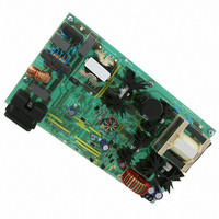
EVAL BOARD FOR NCP1605FORWG
Manufacturer
ON Semiconductor
Datasheets
1.NCP1217P100G.pdf
(19 pages)
2.NCP1605ADR2G.pdf
(32 pages)
3.NCP1605FORWGEVB.pdf
(2 pages)
4.NCP1605FORWGEVB.pdf
(20 pages)
Specifications of NCP1605FORWGEVB
Design Resources
NCP1605FORWGEVB BOM NCP1605FORWGEVB Gerber Files NCP1605 EVB Schematic
Main Purpose
AC/DC, Primary and Secondary Side with PFC
Outputs And Type
1, Isolated
Voltage - Output
19V
Current - Output
8A
Voltage - Input
90 ~ 265VAC
Regulator Topology
Forward Converter
Frequency - Switching
133kHz
Board Type
Fully Populated
Utilized Ic / Part
NCP1217, NCP1605
Lead Free Status / RoHS Status
Lead free / RoHS Compliant
Power - Output
-
Lead Free Status / Rohs Status
Lead free / RoHS Compliant
For Use With/related Products
NCP1605FORWG
Other names
NCP1605FORWGEVBOS


− Latched off of the circuit (when the “STDWN” pin,
voltage is properly and safely regulated. “pfcOK/REF5V”
should be used to allow operation of the downstream
converter.
Standby Management
when the power demand drops below a given level. This is
absorption of the line current necessary for matching the load
power demand. When the voltage applied to Pin 1 goes below
300 mV:
•
•
•
And “pfcOK/REF5V” is high when the PFC output
The NCP1605(A) automatically skips switching cycles
In normal operation, the circuit controls the continuous
The output pulses are blanked and Pin 3
(“V
The output of the PFC stage being not fed any more, it
drops. When the output voltage goes below 95.5% of
the regulation level, the circuit resumes operation until
“FLAG1” becomes low (what means that the output
voltage has exceeded the regulation level).
At that moment, if V
skipping phase starts.
V
Pin13
CONTROL
Standby Input
, exceeds 2.5 V).
Voltage
”) is grounded.
NCP1605
Pin1
1
2
3
4 13
5
6
7
8
16
15
14
12
10
11
Rectified
AC line
9
is still below 300 mV, a new
C
V
+
CC
Figure 63. Signal for Standby Detection
PFC stage
http://onsemi.com
downstream converter
Feed−back of the
24
+
accomplished by monitoring the Pin 1 voltage that must
receive a voltage below 300 mV in light load conditions.
Practically, a portion of the feedback signal of the
downstream converter (or some other signal able to indicate
that the power demand is low) should be applied to Pin 1.
output with a small amount of power, the circuit operates
from time to time at a higher power level. As an example
and to make it simple, instead of continuously supplying
1% of P
P
cycle mode, also named controlled burst operation. This
burst operation is much more efficient compared to a
continuous power flow as it drastically reduces the number
of pulsations and therefore the switching losses associated
to them.
MAX
In other words, instead of continuously providing the
for 10% of the time. The IC enters the so−called skip
MAX
, the circuit can provide the load with 10% of
controller
downstream converter
SMPS
Related parts for NCP1605FORWGEVB
Image
Part Number
Description
Manufacturer
Datasheet
Request
R

Part Number:
Description:
ON Semiconductor [VOLTAGE REGULATOR]
Manufacturer:
ON Semiconductor
Datasheet:
Part Number:
Description:
357-036-542-201 CARDEDGE 36POS DL .156 BLK LOPRO
Manufacturer:
ON Semiconductor
Datasheet:
Part Number:
Description:
357-036-542-201 CARDEDGE 36POS DL .156 BLK LOPRO
Manufacturer:
ON Semiconductor
Datasheet:
Part Number:
Description:
357-036-542-201 CARDEDGE 36POS DL .156 BLK LOPRO
Manufacturer:
ON Semiconductor
Datasheet:
Part Number:
Description:
357-036-542-201 CARDEDGE 36POS DL .156 BLK LOPRO
Manufacturer:
ON Semiconductor
Datasheet:
Part Number:
Description:
357-036-542-201 CARDEDGE 36POS DL .156 BLK LOPRO
Manufacturer:
ON Semiconductor
Datasheet:
Part Number:
Description:
357-036-542-201 CARDEDGE 36POS DL .156 BLK LOPRO
Manufacturer:
ON Semiconductor
Datasheet:
Part Number:
Description:
357-036-542-201 CARDEDGE 36POS DL .156 BLK LOPRO
Manufacturer:
ON Semiconductor
Datasheet:
Part Number:
Description:
357-036-542-201 CARDEDGE 36POS DL .156 BLK LOPRO
Manufacturer:
ON Semiconductor
Datasheet:
Part Number:
Description:
357-036-542-201 CARDEDGE 36POS DL .156 BLK LOPRO
Manufacturer:
ON Semiconductor
Datasheet:
Part Number:
Description:
357-036-542-201 CARDEDGE 36POS DL .156 BLK LOPRO
Manufacturer:
ON Semiconductor
Datasheet:
Part Number:
Description:
Manufacturer:
ON Semiconductor
Datasheet:
Part Number:
Description:
Manufacturer:
ON Semiconductor
Datasheet:
Part Number:
Description:
Manufacturer:
ON Semiconductor
Datasheet: