NCP1605FORWGEVB ON Semiconductor, NCP1605FORWGEVB Datasheet - Page 28
NCP1605FORWGEVB
Manufacturer Part Number
NCP1605FORWGEVB
Description
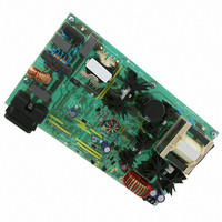
EVAL BOARD FOR NCP1605FORWG
Manufacturer
ON Semiconductor
Datasheets
1.NCP1217P100G.pdf
(19 pages)
2.NCP1605ADR2G.pdf
(32 pages)
3.NCP1605FORWGEVB.pdf
(2 pages)
4.NCP1605FORWGEVB.pdf
(20 pages)
Specifications of NCP1605FORWGEVB
Design Resources
NCP1605FORWGEVB BOM NCP1605FORWGEVB Gerber Files NCP1605 EVB Schematic
Main Purpose
AC/DC, Primary and Secondary Side with PFC
Outputs And Type
1, Isolated
Voltage - Output
19V
Current - Output
8A
Voltage - Input
90 ~ 265VAC
Regulator Topology
Forward Converter
Frequency - Switching
133kHz
Board Type
Fully Populated
Utilized Ic / Part
NCP1217, NCP1605
Lead Free Status / RoHS Status
Lead free / RoHS Compliant
Power - Output
-
Lead Free Status / Rohs Status
Lead free / RoHS Compliant
For Use With/related Products
NCP1605FORWG
Other names
NCP1605FORWGEVBOS


More specifically, when the circuit is in OFF state:
•
•
•
•
V
⇒ the circuit enters the
working phase
V
⇒ the circuit enters the
latched−off phase
V
⇒ the circuit enters the
startup phase
V
⇒ the circuit resets
The figures on the following pages portray the circuit behavior during a startup phase:
The drive output is kept low
All the blocks are off except:
In case of normal conditions (Figure 70).
As a function of the brown−out pin voltage (Figure 71).
CC
CC
CC
CC
1. The UVLO circuitry that keeps monitoring the
2. The TSD (thermal shutdown)
3. The “STDWN” latch that stores its output state.
4. The Undervoltage Protection (“UVP”).
5. The brown−out circuitry. One must note that the
6. The high voltage, startup current source when the
goes below V
exceeds V
drops below V
goes below V
V
V
source accordingly.
comparator is reset during the latched−off phase
so that its threshold is the upper one (1 V) when
the circuit enters the active phase (refer to next
“V
circuit is in startup phase (that is when V
lower than V
CC
CC
CC
Conditions
voltage and controlling the startup current
sequences” section).
CC
CC
ON
CC
CC
RESET
STUP
CC
OFF
STUP).
The startup current source is disabled
The circuit is fully active
The circuit is in OFF state
The brown−out block resets during the
latched−off phase so that its comparator
threshold is forced to be the upper one (1 V)
The high voltage, startup current source turns
on to charge V
The drive output and the “pfcOK” are in low
state (the circuit is off)
All the circuit blocks are reset except:
The high voltage, startup current source is on.
The whole circuitry is reset including the
“TSD” and the “STDWN” latch. After reset,
the TSD threshold is 150°C and the output of
the “STDWN latch” is low.
(no condition forces the circuit off)
The thermal shutdown (TSD) and the
brown−out block that keep operating
The “STDWN” latch.
CC
“OFF” is Low
.
CC
http://onsemi.com
is
28
•
•
•
V
in accordance to the V
CC
The following table summarizes the state of the circuit
The Pin 3 capacitor is discharged and kept grounded
along the OFF time, to initialize it for the next
operating sequence, where it must be slowly and
gradually charged to offer some soft−start.
The “pfcOK” pin is grounded.
The output of the “V
grounded
Sequences
The startup current source is disabled
The circuit is in OFF state
The circuit is in OFF state
The brown−out block resets during the latched−off
phase so that its comparator threshold is forced to be
the upper one (1 V)
The high voltage, startup current source turns on to
charge V
The drive output and the “pfcOK” are in low state (the
circuit is off)
All the circuit blocks are reset except:
The high voltage, startup current source is on.
The whole circuitry is reset including the “TSD” and the
“STDWN” latch. After reset, the TSD threshold is 150°C
and the output of the “STDWN latch” is low.
(due to some protection like the thermal shutdown)
The thermal shutdown (TSD) and the brown−out
block that keep operating
The “STDWN” latch.
CC
.
CC
TON
“OFF” is High
level.
processing block” is
Related parts for NCP1605FORWGEVB
Image
Part Number
Description
Manufacturer
Datasheet
Request
R

Part Number:
Description:
ON Semiconductor [VOLTAGE REGULATOR]
Manufacturer:
ON Semiconductor
Datasheet:
Part Number:
Description:
357-036-542-201 CARDEDGE 36POS DL .156 BLK LOPRO
Manufacturer:
ON Semiconductor
Datasheet:
Part Number:
Description:
357-036-542-201 CARDEDGE 36POS DL .156 BLK LOPRO
Manufacturer:
ON Semiconductor
Datasheet:
Part Number:
Description:
357-036-542-201 CARDEDGE 36POS DL .156 BLK LOPRO
Manufacturer:
ON Semiconductor
Datasheet:
Part Number:
Description:
357-036-542-201 CARDEDGE 36POS DL .156 BLK LOPRO
Manufacturer:
ON Semiconductor
Datasheet:
Part Number:
Description:
357-036-542-201 CARDEDGE 36POS DL .156 BLK LOPRO
Manufacturer:
ON Semiconductor
Datasheet:
Part Number:
Description:
357-036-542-201 CARDEDGE 36POS DL .156 BLK LOPRO
Manufacturer:
ON Semiconductor
Datasheet:
Part Number:
Description:
357-036-542-201 CARDEDGE 36POS DL .156 BLK LOPRO
Manufacturer:
ON Semiconductor
Datasheet:
Part Number:
Description:
357-036-542-201 CARDEDGE 36POS DL .156 BLK LOPRO
Manufacturer:
ON Semiconductor
Datasheet:
Part Number:
Description:
357-036-542-201 CARDEDGE 36POS DL .156 BLK LOPRO
Manufacturer:
ON Semiconductor
Datasheet:
Part Number:
Description:
357-036-542-201 CARDEDGE 36POS DL .156 BLK LOPRO
Manufacturer:
ON Semiconductor
Datasheet:
Part Number:
Description:
Manufacturer:
ON Semiconductor
Datasheet:
Part Number:
Description:
Manufacturer:
ON Semiconductor
Datasheet:
Part Number:
Description:
Manufacturer:
ON Semiconductor
Datasheet: