NCP1605FORWGEVB ON Semiconductor, NCP1605FORWGEVB Datasheet - Page 16
NCP1605FORWGEVB
Manufacturer Part Number
NCP1605FORWGEVB
Description
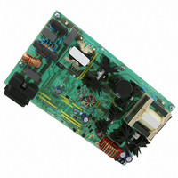
EVAL BOARD FOR NCP1605FORWG
Manufacturer
ON Semiconductor
Datasheets
1.NCP1217P100G.pdf
(19 pages)
2.NCP1605ADR2G.pdf
(32 pages)
3.NCP1605FORWGEVB.pdf
(2 pages)
4.NCP1605FORWGEVB.pdf
(20 pages)
Specifications of NCP1605FORWGEVB
Design Resources
NCP1605FORWGEVB BOM NCP1605FORWGEVB Gerber Files NCP1605 EVB Schematic
Main Purpose
AC/DC, Primary and Secondary Side with PFC
Outputs And Type
1, Isolated
Voltage - Output
19V
Current - Output
8A
Voltage - Input
90 ~ 265VAC
Regulator Topology
Forward Converter
Frequency - Switching
133kHz
Board Type
Fully Populated
Utilized Ic / Part
NCP1217, NCP1605
Lead Free Status / RoHS Status
Lead free / RoHS Compliant
Power - Output
-
Lead Free Status / Rohs Status
Lead free / RoHS Compliant
For Use With/related Products
NCP1605FORWG
Other names
NCP1605FORWGEVBOS


CSout
V
STBY
Stdwn
CSin
BO /
OVP
control
FB
Ct
95.5% V
+
300 mV
V
ovp
12% V
Ics
1 V / 0.5 V
ref
-
+
FLAG1
V/I
= V
Ich=K.Iout.Iout
V
STBY
ref
ref
+
-
Error Amplifier
V
V
ref
out
pfcOK
+
-
I
-
+
+
-
out
Low Detect
OFF
SKIP
V
+
-
outL
+
-
V
outL
outON
L
S
R
STBY
BO_NOK
OVP
UVP
±20 mA
Q
100 mV
FLAG1
V
3 V
pfcOK
Ics
STBY
Ics > 250 mA
Fi
+
-
R
50 mV
200 mA
FLAG1
STDWN
OVP
OCP
http://onsemi.com
V
ref
-
+
2.R
51 Bl
V
V
REGUL
SKIP
DD
PWM
Comparator
V
REGUL
-
+
+
-
16
ZCD
DT
OFF
OCP
k Di
OFF
Vcc<VccRST
All the RS latches are
S
RESET dominant
OVP
processing
outON
TSD
Shutdown
circuitry
Thermal
R
S
Internal
BO_NOK
R
Vton
STDWN
R
R
Lstup
Dead−time
S
R
Detection
S
Q
R
CLK
Latch
PWM
Latch
SKIP
stdwn
Ct_OK
R
Q
Q
Q
UVP
Management
UVLO (Vcc<VccOFF)
UVLO
V
outON
FAULT
t(on)
Synchronization
V
V
HVCS_ON
I
Oscillator /
DD
ref
ref
Block
REF5V
UVLOs
Reset
Latch
DT
Regul
HVCS_ON
OFF
ZCD
V
pfcOK
CC
Output
Buffer
pfcOK /
REF5V
OSC /
SYNC
V
GND
HV
NC
Drv
CC
Related parts for NCP1605FORWGEVB
Image
Part Number
Description
Manufacturer
Datasheet
Request
R

Part Number:
Description:
ON Semiconductor [VOLTAGE REGULATOR]
Manufacturer:
ON Semiconductor
Datasheet:
Part Number:
Description:
357-036-542-201 CARDEDGE 36POS DL .156 BLK LOPRO
Manufacturer:
ON Semiconductor
Datasheet:
Part Number:
Description:
357-036-542-201 CARDEDGE 36POS DL .156 BLK LOPRO
Manufacturer:
ON Semiconductor
Datasheet:
Part Number:
Description:
357-036-542-201 CARDEDGE 36POS DL .156 BLK LOPRO
Manufacturer:
ON Semiconductor
Datasheet:
Part Number:
Description:
357-036-542-201 CARDEDGE 36POS DL .156 BLK LOPRO
Manufacturer:
ON Semiconductor
Datasheet:
Part Number:
Description:
357-036-542-201 CARDEDGE 36POS DL .156 BLK LOPRO
Manufacturer:
ON Semiconductor
Datasheet:
Part Number:
Description:
357-036-542-201 CARDEDGE 36POS DL .156 BLK LOPRO
Manufacturer:
ON Semiconductor
Datasheet:
Part Number:
Description:
357-036-542-201 CARDEDGE 36POS DL .156 BLK LOPRO
Manufacturer:
ON Semiconductor
Datasheet:
Part Number:
Description:
357-036-542-201 CARDEDGE 36POS DL .156 BLK LOPRO
Manufacturer:
ON Semiconductor
Datasheet:
Part Number:
Description:
357-036-542-201 CARDEDGE 36POS DL .156 BLK LOPRO
Manufacturer:
ON Semiconductor
Datasheet:
Part Number:
Description:
357-036-542-201 CARDEDGE 36POS DL .156 BLK LOPRO
Manufacturer:
ON Semiconductor
Datasheet:
Part Number:
Description:
Manufacturer:
ON Semiconductor
Datasheet:
Part Number:
Description:
Manufacturer:
ON Semiconductor
Datasheet:
Part Number:
Description:
Manufacturer:
ON Semiconductor
Datasheet: