NCP1605FORWGEVB ON Semiconductor, NCP1605FORWGEVB Datasheet - Page 22
NCP1605FORWGEVB
Manufacturer Part Number
NCP1605FORWGEVB
Description
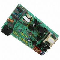
EVAL BOARD FOR NCP1605FORWG
Manufacturer
ON Semiconductor
Datasheets
1.NCP1217P100G.pdf
(19 pages)
2.NCP1605ADR2G.pdf
(32 pages)
3.NCP1605FORWGEVB.pdf
(2 pages)
4.NCP1605FORWGEVB.pdf
(20 pages)
Specifications of NCP1605FORWGEVB
Design Resources
NCP1605FORWGEVB BOM NCP1605FORWGEVB Gerber Files NCP1605 EVB Schematic
Main Purpose
AC/DC, Primary and Secondary Side with PFC
Outputs And Type
1, Isolated
Voltage - Output
19V
Current - Output
8A
Voltage - Input
90 ~ 265VAC
Regulator Topology
Forward Converter
Frequency - Switching
133kHz
Board Type
Fully Populated
Utilized Ic / Part
NCP1217, NCP1605
Lead Free Status / RoHS Status
Lead free / RoHS Compliant
Power - Output
-
Lead Free Status / Rohs Status
Lead free / RoHS Compliant
For Use With/related Products
NCP1605FORWG
Other names
NCP1605FORWGEVBOS


The propagation delay (V
output high) is in the range of 300 ns, typically.
The Zero Current Detection:
•
•
Remarks:
•
Is used to detect the dead−time sequences (“DT” high)
and hence, to process (V
output (V
the on−time modulation block.
Prevents the MOSFET from turning on as long as the
“DT” and “ZCD” signals are low. This is the case as
long as some current flows through the coil. This
delaying action on the output stage tends to make the
MOSFET turn on at the valley. To further optimize the
valley switching, one can apply the voltage of an
auxiliary winding to Pin 6 (CS
compared to an internal 100 mV reference, so that
ZCD turns high only if (V
A resistor can be placed between Pin 6 and ground to
increase the ZCD precision.
Filter
EMI
R
sense
CONTROL
R
V
ocp
in
C
). In other words, this is an input of
CS
in
5
in
Pin6
The CS block performs the overcurrent protection and the zero current detection.
TON
Pin6
V
(I COIL )zcd +
lower than 100 mV) to (drive
Icoil
dd
) from the error amplifier
< 100 mV).
OUT
Current Mirror
). The voltage is
Ics
V
dd
R pin6 @ R CS
Figure 60. Current Sense Block
I
Ics
cs
R OCP
> 250 mA ≥ OCP
6
Icoil
100 mV
http://onsemi.com
CS
Rzcd
out
Rdrv
(RESET of the PWM latch)
+
-
100 mV +
22
•
•
It is recommended to:
OCP
outON
Vzcd
It is worth highlighting that the circuit permanently
senses the coil current and that it prevents any turn on
of the power switch as long as the core is not reset.
This feature protects the MOSFET from the possible
excessive stress it could suffer from, if it was allowed
to turn on while a huge current flows through the coil.
In particular, this scheme effectively protects the PFC
stage during the startup phase when huge in−rush
currents charge the output capacitor.
In addition this detection method does not require any
auxiliary winding. A simple coil can then be used in
the PFC stage.
ZCD
R pin6 @ 250 mA
1. Keep R
2. Choose R
than (3 x R
leakage prevents a proper zero current detection.
For instance, if R
exceed 6.6 kW.
100 mV
S
LdT
R
output
OCP
buffer
Q
ZCD
OCP
equal to or lower than 5 kW
@ (I COIL ) MAX +
as high as possible but not bigger
Vcc
). This is to avoid that the Pin 6
OCP
DT
DRV
is 2.2 kW, R
10
400 W
R pin6
L1
M1
ZCD
C
@ (I COIL ) MAX
D1
bulk
should not
Vout
LOAD
Related parts for NCP1605FORWGEVB
Image
Part Number
Description
Manufacturer
Datasheet
Request
R

Part Number:
Description:
ON Semiconductor [VOLTAGE REGULATOR]
Manufacturer:
ON Semiconductor
Datasheet:
Part Number:
Description:
357-036-542-201 CARDEDGE 36POS DL .156 BLK LOPRO
Manufacturer:
ON Semiconductor
Datasheet:
Part Number:
Description:
357-036-542-201 CARDEDGE 36POS DL .156 BLK LOPRO
Manufacturer:
ON Semiconductor
Datasheet:
Part Number:
Description:
357-036-542-201 CARDEDGE 36POS DL .156 BLK LOPRO
Manufacturer:
ON Semiconductor
Datasheet:
Part Number:
Description:
357-036-542-201 CARDEDGE 36POS DL .156 BLK LOPRO
Manufacturer:
ON Semiconductor
Datasheet:
Part Number:
Description:
357-036-542-201 CARDEDGE 36POS DL .156 BLK LOPRO
Manufacturer:
ON Semiconductor
Datasheet:
Part Number:
Description:
357-036-542-201 CARDEDGE 36POS DL .156 BLK LOPRO
Manufacturer:
ON Semiconductor
Datasheet:
Part Number:
Description:
357-036-542-201 CARDEDGE 36POS DL .156 BLK LOPRO
Manufacturer:
ON Semiconductor
Datasheet:
Part Number:
Description:
357-036-542-201 CARDEDGE 36POS DL .156 BLK LOPRO
Manufacturer:
ON Semiconductor
Datasheet:
Part Number:
Description:
357-036-542-201 CARDEDGE 36POS DL .156 BLK LOPRO
Manufacturer:
ON Semiconductor
Datasheet:
Part Number:
Description:
357-036-542-201 CARDEDGE 36POS DL .156 BLK LOPRO
Manufacturer:
ON Semiconductor
Datasheet:
Part Number:
Description:
Manufacturer:
ON Semiconductor
Datasheet:
Part Number:
Description:
Manufacturer:
ON Semiconductor
Datasheet:
Part Number:
Description:
Manufacturer:
ON Semiconductor
Datasheet: