RDK-142 Power Integrations, RDK-142 Datasheet - Page 8
RDK-142
Manufacturer Part Number
RDK-142
Description
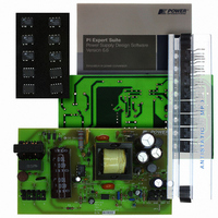
KIT REF DESIGN TOP HX FOR TOP258
Manufacturer
Power Integrations
Series
TOPSwitch®-HXr
Datasheet
1.RDK-142.pdf
(40 pages)
Specifications of RDK-142
Mfg Application Notes
TOPSwitch-HX Family Appl Note
Main Purpose
AC/DC, Primary Side
Outputs And Type
2, Non-Isolated
Power - Output
35W
Voltage - Output
5V, 12V
Current - Output
2.2A, 2A
Voltage - Input
90 ~ 265VAC
Regulator Topology
Flyback
Frequency - Switching
30kHz
Board Type
Fully Populated
Utilized Ic / Part
TOP258
Product
Accessories & Kits
Silicon Manufacturer
Power Integrations
Kit Application Type
Displays
Application Sub Type
LCD Monitor
Kit Contents
Samples, Fully Functional Reference Board And Complete Documentation
Rohs Compliant
Yes
Lead Free Status / RoHS Status
Lead free / RoHS Compliant
Other names
596-1193


as the ratio I
output is then regulated by modulating the switching frequency (variable frequency PWM
control). As the load decreases further, the switching frequency decreases linearly from
full frequency down to 30 kHz.
Once the switching frequency has reached 30 kHz the controller keeps this switching
frequency constant and the peak current is reduced to regulate the output (fixed
frequency, direct duty cycle PWM control).
As the load is further reduced and the ratio I
enter a multi-cycle-modulation mode for excellent efficiency at light load or standby
operation and low no-load input power consumption.
Diode D5, together with R6, R7, C6 and Zener VR1, forms a clamp network that limits the
drain voltage of U1 at the instant of turn-off. Zener VR1 provides a defined maximum
clamp voltage and typically only conducts during fault conditions such as overload. This
allows the RCD clamp (R6, C6 and D5) to be sized for normal operation, thereby
maximizing efficiency at light load. Resistor R7 is required due to the choice of a fast
recovery diode for D5. A fast versus ultra fast recovery diode allows some recovery of
the clamp energy but requires R7 to limit reverse diode current and dampen high
frequency ringing.
The output of the bias winding is rectified by diode D6 and filtered by resistor R10 and
capacitor C10. This rectified and filtered output is used by the optocoupler U2 to provide
the control current to the control terminal of U1.
Should the feedback circuit fail (open loop condition), the output of the power supply will
exceed the regulation limits.
increased voltage at the output of the bias winding. Zener VR2 will break down and
current will flow into the “M” pin of IC U1, thus initiating a hysteretic OVP shutdown with
automatic restart attempts. Resistor R5 limits the current into the M pin; if latching OVP
is desired, the value of R5 can be reduced to 20 Ω.
The output voltage of the power supply is maintained in regulation by the feedback circuit
on the secondary side of the circuit. The feedback circuit controls the output voltage by
changing the optocoupler current. Change in the optocoupler diode current results in a
change of current into the control pin of IC U1.
variation of duty cycle and hence the output voltage of the power supply.
4.3 Output Rectification
Output rectification for the 5 V output is provided by diode D8. Low ESR capacitor C17
provides filtering.
significantly attenuates the switching ripple across C17 and ensures a low ripple output.
Power Integrations
Tel: +1 408 414 9200 Fax: +1 408 414 9201
www.powerint.com
P
/I
LIMITEXT
Inductor L3 and capacitor C18 form a second stage filter that
falls below 55%, the peak drain current is held constant. The
This increased voltage at output will also result in an
P
/I
LIMITEXT
Variation of this current results in
falls below 25%, the controller will
Page 8 of 40
Related parts for RDK-142
Image
Part Number
Description
Manufacturer
Datasheet
Request
R

Part Number:
Description:
KIT REF DESIGN FOR LNK457D
Manufacturer:
Power Integrations
Datasheet:

Part Number:
Description:
REFERENCE DESIGN LINKSWITCH-PH
Manufacturer:
Power Integrations
Datasheet:

Part Number:
Description:
KIT REF DESIGN FOR LNK403EG
Manufacturer:
Power Integrations
Datasheet:

Part Number:
Description:
KIT REF DESIGN FOR LNK406EG
Manufacturer:
Power Integrations
Datasheet:

Part Number:
Description:
KIT REF DESIGN LINKSWITCH-CV
Manufacturer:
Power Integrations
Datasheet:

Part Number:
Description:
KIT REF DESIGN LINKSWITCH 2
Manufacturer:
Power Integrations
Datasheet:

Part Number:
Description:
Specifications: Family: Eval Boards - DC/DC & AC/DC (Off-Line) SMPS ; Series: HiperLCS™ ; Main Purpose: DC/DC, Step Down ; Outputs and Type: 1, Isolated ; Power - Output: 150W ; Voltage - Output: 24V ; Current - Output: 6.25A ; Voltage - Input:
Manufacturer:
Power Integrations, Inc.
Datasheet:

Part Number:
Description:
KIT DESIGN REF TINYSWITCH-III
Manufacturer:
Power Integrations
Datasheet:

Part Number:
Description:
KIT DESIGN REF LINKSWITCH LP
Manufacturer:
Power Integrations
Datasheet:

Part Number:
Description:
KIT REF DESIGN LED LINKSWITCH TN
Manufacturer:
Power Integrations
Datasheet:
Part Number:
Description:
KIT REF DESIGN PG LINKSWITCH-II
Manufacturer:
Power Integrations
Datasheet:
Part Number:
Description:
REFERENCE DESIGN LINKSWITCH-PL
Manufacturer:
Power Integrations
Datasheet:
Part Number:
Description:
REFERENCE DESIGN LINKSWITCH-PH
Manufacturer:
Power Integrations
Datasheet:

Part Number:
Description:
KIT REF DESIGN 36-72W MOTOR DRVR
Manufacturer:
Power Integrations
Datasheet:
Part Number:
Description:
Specifications: Manufacturer: Power Integrations ; Output Voltage: 380 VDC ; Input / Supply Voltage (Max): 264 VAC ; Input / Supply Voltage (Min): 90 VAC ; Mounting Style: Through Hole ; Output Current: 0.913 A ; Output Power: 347 W
Manufacturer:
Power Integrations, Inc.