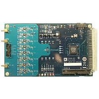
EVAL-AD7689EDZ Analog Devices Inc, EVAL-AD7689EDZ Datasheet - Page 9
EVAL-AD7689EDZ
Manufacturer Part Number
EVAL-AD7689EDZ
Description
BOARD EVAL AD7689
Manufacturer
Analog Devices Inc
Series
PulSAR®r
Specifications of EVAL-AD7689EDZ
Number Of Adc's
1
Number Of Bits
16
Sampling Rate (per Second)
250k
Data Interface
Serial
Inputs Per Adc
8 Single Ended
Input Range
±VREF
Power (typ) @ Conditions
12.5mW @ 250kSPS, 5 V
Voltage Supply Source
Single Supply
Operating Temperature
-40°C ~ 85°C
Utilized Ic / Part
AD7689
Silicon Manufacturer
Analog Devices
Application Sub Type
ADC
Kit Application Type
Data Converter
Silicon Core Number
AD7689
Lead Free Status / RoHS Status
Lead free / RoHS Compliant


PIN CONFIGURATIONS AND FUNCTION DESCRIPTIONS
Table 7. Pin Function Descriptions
Pin No.
1, 20
2
3
4, 5
6
7
8
9
10
11
12
13
AD7682
Mnemonic
VDD
REF
REFIN
GND
NC
IN2
NC
IN3
COM
CNV
DIN
SCK
REFIN
NOTES
1. NC = NO CONNECT.
2. THE EXPOSED PAD IS NOT CONNECTED
GND
GND
VDD
REF
INTERNALLY. FOR INCREASED
RELIABILITY OF THE SOLDER JOINTS, IT
IS RECOMMENDED THAT THE PAD BE
SOLDERED TO THE SYSTEM
GROUND PLANE.
Figure 4. AD7682 Pin Configuration
1
2
3
4
5
(Not to Scale)
AD7682
TOP VIEW
AD7689
Mnemonic
VDD
REF
REFIN
GND
IN4
IN5
IN6
IN7
COM
CNV
DIN
SCK
PIN 1
INDICATOR
15 VIO
14 SDO
13 SCK
12 DIN
11 CNV
Type
P
AI/O
AI/O
P
AI
AI
AI
AI
AI
DI
DI
DI
1
Description
Power Supply. Nominally 2.5 V to 5.5 V when using an external reference and decoupled
with 10 μF and 100 nF capacitors.
When using the internal reference for a2.5 V output, the minimum should be 3.0 V.
When using the internal reference for 4.096 V output, the minimum should be 4.6 V.
Reference Input/Output. See the Voltage Reference Output/Input section.
When the internal reference is enabled, this pin produces a selectable system reference of
2.5 V or 4.096 V.
When the internal reference is disabled and the buffer is enabled, REF produces a
buffered version of the voltage present on the REFIN pin (VDD − 0.5 V maximum), which
is useful when using low cost, low power references.
For improved drift performance, connect a precision reference to REF (0.5 V to VDD).
For any reference method, this pin needs decoupling with an external 10 μF capacitor
connected as close to REF as possible. See the Reference Decoupling section.
Internal Reference Output/Reference Buffer Input. See the Voltage Reference
Output/Input section.
When using the internal reference, the internal unbuffered reference voltage is present
and needs decoupling with a 0.1 μF capacitor.
When using the internal reference buffer, apply a source between 0.5 V and (VDD − 0.5 V)
that is buffered to the REF pin, as described in the REF pin description.
Power Supply Ground.
AD7682: no connection.
AD7689: Analog Input Channel 4.
AD7682: Analog Input Channel 2.
AD7689: Analog Input Channel 5.
AD7682: no connection.
AD7689: Analog Input Channel 6.
AD7682: Analog Input Channel 3.
AD7689: Analog Input Channel 7.
Common Channel Input. All input channels, IN[7:0], can be referenced to a common-
mode point of 0 V or V
Conversion Input. On the rising edge, CNV initiates the conversion. During conversion, if
CNV is held low, the busy indictor is enabled.
Data Input. This input is used for writing to the 14-bit configuration register. The
configuration register can be written to during and after conversion.
Serial Data Clock Input. This input is used to clock out the data on SDO and clock in data
on DIN in an MSB first fashion.
Rev. B | Page 9 of 32
REF
/2 V.
REFIN
NOTES
1. THE EXPOSED PAD IS NOT CONNECTED
GND
GND
VDD
REF
INTERNALLY. FOR INCREASED
RELIABILITY OF THE SOLDER JOINTS, IT
IS RECOMMENDED THAT THE PAD BE
SOLDERED TO THE SYSTEM
GROUND PLANE.
Figure 5. AD7689 Pin Configuration
1
2
3
4
5
(Not to Scale)
AD7689
TOP VIEW
PIN 1
INDICATOR
15 VIO
14 SDO
13 SCK
12 DIN
11 CNV
AD7682/AD7689
Related parts for EVAL-AD7689EDZ
Image
Part Number
Description
Manufacturer
Datasheet
Request
R


Part Number:
Description:
BOARD EVAL FOR SI270X-A
Manufacturer:
Silicon Laboratories Inc
Datasheet:

Part Number:
Description:
BUCK CONV REF DESIGN KIT IP1201
Manufacturer:
International Rectifier
Datasheet:
Part Number:
Description:
BOARD DEMO SYNC DUAL BUCK CNVTER
Manufacturer:
International Rectifier
Datasheet:
Part Number:
Description:
BOARD DEMO SYNC BUCK CONVETER
Manufacturer:
International Rectifier
Datasheet:

Part Number:
Description:
EVALBOARD/EB Omnidirectional microphone - Analog
Manufacturer:
Analog Devices
Datasheet:
Part Number:
Description:
EVALBOARD/EB Omnidirectional microphone - Analog
Manufacturer:
Analog Devices
Datasheet:


Part Number:
Description:
BOARD EVAL LED DRIVER LT3756
Manufacturer:
Linear Technology
Datasheet:

Part Number:
Description:
BOARD EVAL FOR AD7741/7742
Manufacturer:
Analog Devices Inc
Datasheet:

Part Number:
Description:
±1.7g Dual-Axis IMEMS Accelerometer Evaluation Board
Manufacturer:
Analog Devices Inc
Datasheet:

Part Number:
Description:
IC MULTIPLIER ANALOG 8-SOIC T/R
Manufacturer:
Analog Devices Inc
Datasheet:

Part Number:
Description:
IC ANALOG MULTIPLIER 8-DIP
Manufacturer:
Analog Devices Inc
Datasheet:
Part Number:
Description:
IC ANALOG MULTIPLIER 8-SOIC
Manufacturer:
Analog Devices Inc
Datasheet:
Part Number:
Description:
IC ANALOG MULTIPLIER 8-DIP
Manufacturer:
Analog Devices Inc
Datasheet: