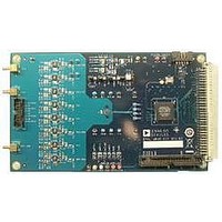
EVAL-AD7689EDZ Analog Devices Inc, EVAL-AD7689EDZ Datasheet - Page 19
EVAL-AD7689EDZ
Manufacturer Part Number
EVAL-AD7689EDZ
Description
BOARD EVAL AD7689
Manufacturer
Analog Devices Inc
Series
PulSAR®r
Specifications of EVAL-AD7689EDZ
Number Of Adc's
1
Number Of Bits
16
Sampling Rate (per Second)
250k
Data Interface
Serial
Inputs Per Adc
8 Single Ended
Input Range
±VREF
Power (typ) @ Conditions
12.5mW @ 250kSPS, 5 V
Voltage Supply Source
Single Supply
Operating Temperature
-40°C ~ 85°C
Utilized Ic / Part
AD7689
Silicon Manufacturer
Analog Devices
Application Sub Type
ADC
Kit Application Type
Data Converter
Silicon Core Number
AD7689
Lead Free Status / RoHS Status
Lead free / RoHS Compliant


Input Configurations
Figure 30 shows the different methods for configuring the analog
inputs with the configuration register, CFG[12:10]. Refer to the
Configuration Register, CFG, section for more details.
The analog inputs can be configured as
•
•
•
•
Figure 30A, single-ended referenced to system ground;
CFG[12:10] = 111
In this configuration, all inputs (IN[7:0]) have a range of
GND to V
Figure 30B, bipolar differential with a common reference
point; COM = V
Unipolar differential with COM connected to a ground
sense; CFG[12:10] = 110
In this configuration, all inputs IN[7:0] have a range of
GND to V
Figure 30C, bipolar differential pairs with the negative
input channel referenced to V
Unipolar differential pairs with the negative input channel
referenced to a ground sense; CFG[12:10] = 10X
In these configurations, the positive input channels have
the range of GND to V
a sense referred to V
unipolar pairs. The positive channel is configured with
CFG[9:7]. If CFG[9:7] is even, then IN0, IN2, IN4, and IN6
are used. If CFG[9:7] is odd, then IN1, IN3, IN5, and IN7
are used, as indicated by the channels with parentheses in
Figure 30C. For example, for IN0/IN1 pairs with the
positive channel on IN0, CFG[9:7] = 000
pairs with the positive channel on IN5, CFG[9:7] = 101
Note that for the sequencer, detailed in the Channel
Sequencer section, the positive channels are always IN0,
IN2, IN4, and IN6.
Figure 30D, inputs configured in any of the preceding
combinations (showing that the AD7682/AD7689 can be
configured dynamically).
REF
REF
.
.
REF
2
.
/2; CFG[12:10] = 010
REF
REF
/2 for bipolar pairs, or GND for
2
.
. The negative input channels are
REF
/2; CFG[12:10] = 00X
2
2
.
. For IN4/IN5
2
.
2
.
2
Rev. B | Page 19 of 32
.
Sequencer
The AD7682/AD7689 include a channel sequencer useful for
scanning channels in a repeated fashion. Refer to the Channel
Sequencer section for further details of the sequencer operation.
Source Resistance
When the source impedance of the driving circuit is low, the
AD7682/AD7689 can be driven directly. Large source imped-
ances significantly affect the ac performance, especially THD.
The dc performances are less sensitive to the input impedance.
The maximum source impedance depends on the amount of
THD that can be tolerated. The THD degrades as a function of
the source impedance and the maximum input frequency.
CH0+ (–)
CH0– (+)
CH1+ (–)
CH1– (+)
CH2+ (–)
CH2– (+)
CH3+ (–)
CH3– (+)
CH0+
CH1+
CH2+
CH3+
CH4+
CH5+
CH6+
CH7+
Figure 30. Multiplexed Analog Input Configurations
A—8 CHANNELS,
C—4 CHANNELS,
SINGLE ENDED
DIFFERENTIAL
COM
COM
IN2
IN3
IN5
IN7
GND
IN2
IN3
IN5
IN7
GND
IN0
IN1
IN4
IN6
IN0
IN1
IN4
IN6
CH0+ (–)
CH0– (+)
CH1+ (–)
CH1– (+)
COM–
COM–
CH3+
CH2+
CH3+
CH4+
CH5+
CH1+
CH2+
CH4+
CH5+
CH0+
CH6+
CH7+
COMMON REFERNCE
AD7682/AD7689
D—COMBINATION
B—8 CHANNELS,
IN2
IN3
IN5
IN7
COM
COM
GND
IN0
IN1
IN4
IN6
GND
IN2
IN3
IN5
IN7
IN0
IN1
IN4
IN6
Related parts for EVAL-AD7689EDZ
Image
Part Number
Description
Manufacturer
Datasheet
Request
R


Part Number:
Description:
BOARD EVAL FOR SI270X-A
Manufacturer:
Silicon Laboratories Inc
Datasheet:

Part Number:
Description:
BUCK CONV REF DESIGN KIT IP1201
Manufacturer:
International Rectifier
Datasheet:
Part Number:
Description:
BOARD DEMO SYNC DUAL BUCK CNVTER
Manufacturer:
International Rectifier
Datasheet:
Part Number:
Description:
BOARD DEMO SYNC BUCK CONVETER
Manufacturer:
International Rectifier
Datasheet:

Part Number:
Description:
EVALBOARD/EB Omnidirectional microphone - Analog
Manufacturer:
Analog Devices
Datasheet:
Part Number:
Description:
EVALBOARD/EB Omnidirectional microphone - Analog
Manufacturer:
Analog Devices
Datasheet:


Part Number:
Description:
BOARD EVAL LED DRIVER LT3756
Manufacturer:
Linear Technology
Datasheet:

Part Number:
Description:
BOARD EVAL FOR AD7741/7742
Manufacturer:
Analog Devices Inc
Datasheet:

Part Number:
Description:
±1.7g Dual-Axis IMEMS Accelerometer Evaluation Board
Manufacturer:
Analog Devices Inc
Datasheet:

Part Number:
Description:
IC MULTIPLIER ANALOG 8-SOIC T/R
Manufacturer:
Analog Devices Inc
Datasheet:

Part Number:
Description:
IC ANALOG MULTIPLIER 8-DIP
Manufacturer:
Analog Devices Inc
Datasheet:
Part Number:
Description:
IC ANALOG MULTIPLIER 8-SOIC
Manufacturer:
Analog Devices Inc
Datasheet:
Part Number:
Description:
IC ANALOG MULTIPLIER 8-DIP
Manufacturer:
Analog Devices Inc
Datasheet: