EVAL-AD7689EDZ Analog Devices Inc, EVAL-AD7689EDZ Datasheet - Page 24
EVAL-AD7689EDZ
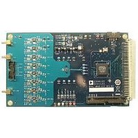
Manufacturer Part Number
EVAL-AD7689EDZ
Description
BOARD EVAL AD7689
Manufacturer
Analog Devices Inc
Series
PulSAR®r
Specifications of EVAL-AD7689EDZ
Number Of Adc's
1
Number Of Bits
16
Sampling Rate (per Second)
250k
Data Interface
Serial
Inputs Per Adc
8 Single Ended
Input Range
±VREF
Power (typ) @ Conditions
12.5mW @ 250kSPS, 5 V
Voltage Supply Source
Single Supply
Operating Temperature
-40°C ~ 85°C
Utilized Ic / Part
AD7689
Silicon Manufacturer
Analog Devices
Application Sub Type
ADC
Kit Application Type
Data Converter
Silicon Core Number
AD7689
Lead Free Status / RoHS Status
Lead free / RoHS Compliant


AD7682/AD7689
The register can be written to during conversion, during acquisi-
tion, or spanning acquisition/conversion, and is updated at the end
of conversion, t
delay when writing the CFG register. Note that, at power-up, the
CFG register is undefined and two dummy conversions are
required to update the register. To preload the CFG register with a
factory setting, hold DIN high for two conversions. Thus
CFG[13:0] = 0x3FFF. This sets the AD7682/AD7689 for the
following:
13
CFG
Table 10. Configuration Register Description
Bit(s)
[13]
[12:10]
[9:7]
[6]
[5:3]
[2:1]
[0]
1
X = don’t care.
Name
CFG
INCC
INx
BW
REF
SEQ
RB
12
INCC
CONV
Description
Configuration update.
0 = keep current configuration settings.
1 = overwrite contents of register.
Input channel configuration. Selection of pseudo bipolar, pseudo differential, pairs, single-ended, or temperature sensor. Refer
to the
Bit 12
0
0
0
1
1
1
Input channel selection in binary fashion.
Bit 9
X
X
X
X
Select bandwidth for low-pass filter. Refer to the
0 = ¼ of BW, uses an additional series resistor to further bandwidth limit the noise. Maximum throughput must also be reduced to ¼.
1 = full BW.
Reference/buffer selection. Selection of internal, external, external buffered, and enabling of the on-chip temperature sensor.
Refer to the
Bit 5
0
0
0
0
1
1
Channel sequencer. Allows for scanning channels in an IN0 to IN[7:0] fashion. Refer to the
Bit 2
0
0
1
1
Read back the CFG register.
0 = read back current configuration at end of data.
1 = do not read back contents of configuration.
(maximum). There is always a one deep
1
1
1
1
11
INCC
Input Configurations
Voltage Reference Output/Input
Bit 11
0
1
1
0
1
1
Bit 8
0
0
1
1
Bit 4
0
0
1
1
1
1
Bit 1
0
1
0
1
10
INCC
AD7682
section.
9
INx
Bit 10
X
0
1
X
0
1
Bit 7
0
1
0
1
Bit 3
0
1
0
1
0
1
1
1
8
INx
Rev. B | Page 24 of 32
section.
Function
Bipolar differential pairs; INx− referenced to V
Bipolar; INx referenced to COM = V
Temperature sensor.
Unipolar differential pairs; INx− referenced to GND ± 0.1 V.
Unipolar, INx referenced to COM = GND ± 0.1 V.
Unipolar, INx referenced to GND.
Channel
IN0
IN1
IN2
IN3
Function
Internal reference, REF = 2.5 V output.
Internal reference, REF = 4.096 V output.
External reference, temperature enabled.
External reference, internal buffer, temperature enabled.
External reference, temperature disabled.
External reference, internal buffer, temperature disabled.
Function
Disable sequencer.
Update configuration during sequence.
Scan IN0 to IN[7:0] (set in CFG[9:7]), then temperature.
Scan IN0 to IN[7:0] (set in CFG[9:7]).
Selectable Low-Pass Filter
7
INx
Bit 9
0
0
…
1
•
•
•
•
•
Table 10 summarizes the configuration register bit details. See
the Theory of Operation section for more details.
6
BW
IN[7:0] unipolar referenced to GND, sequenced in order
Full bandwidth for a one-pole filter
Internal reference/temperature sensor disabled, buffer
enabled
Enables the internal sequencer
No readback of the CFG register
5
REF
Bit 8
0
0
…
1
section.
4
REF
REF
Bit 7
0
1
…
1
/2 ± 0.1 V.
Channel Sequencer
AD7689
3
REF
REF
/2 ± 0.1 V.
Channel
IN0
IN1
…
IN7
2
SEQ
section.
1
SEQ
RB
0
Related parts for EVAL-AD7689EDZ
Image
Part Number
Description
Manufacturer
Datasheet
Request
R


Part Number:
Description:
BOARD EVAL FOR SI270X-A
Manufacturer:
Silicon Laboratories Inc
Datasheet:

Part Number:
Description:
BUCK CONV REF DESIGN KIT IP1201
Manufacturer:
International Rectifier
Datasheet:
Part Number:
Description:
BOARD DEMO SYNC DUAL BUCK CNVTER
Manufacturer:
International Rectifier
Datasheet:
Part Number:
Description:
BOARD DEMO SYNC BUCK CONVETER
Manufacturer:
International Rectifier
Datasheet:

Part Number:
Description:
EVALBOARD/EB Omnidirectional microphone - Analog
Manufacturer:
Analog Devices
Datasheet:
Part Number:
Description:
EVALBOARD/EB Omnidirectional microphone - Analog
Manufacturer:
Analog Devices
Datasheet:


Part Number:
Description:
BOARD EVAL LED DRIVER LT3756
Manufacturer:
Linear Technology
Datasheet:

Part Number:
Description:
BOARD EVAL FOR AD7741/7742
Manufacturer:
Analog Devices Inc
Datasheet:

Part Number:
Description:
±1.7g Dual-Axis IMEMS Accelerometer Evaluation Board
Manufacturer:
Analog Devices Inc
Datasheet:

Part Number:
Description:
IC MULTIPLIER ANALOG 8-SOIC T/R
Manufacturer:
Analog Devices Inc
Datasheet:

Part Number:
Description:
IC ANALOG MULTIPLIER 8-DIP
Manufacturer:
Analog Devices Inc
Datasheet:
Part Number:
Description:
IC ANALOG MULTIPLIER 8-SOIC
Manufacturer:
Analog Devices Inc
Datasheet:
Part Number:
Description:
IC ANALOG MULTIPLIER 8-DIP
Manufacturer:
Analog Devices Inc
Datasheet: