EVAL-AD7689EDZ Analog Devices Inc, EVAL-AD7689EDZ Datasheet - Page 26
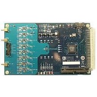
EVAL-AD7689EDZ
Manufacturer Part Number
EVAL-AD7689EDZ
Description
BOARD EVAL AD7689
Manufacturer
Analog Devices Inc
Series
PulSAR®r
Specifications of EVAL-AD7689EDZ
Number Of Adc's
1
Number Of Bits
16
Sampling Rate (per Second)
250k
Data Interface
Serial
Inputs Per Adc
8 Single Ended
Input Range
±VREF
Power (typ) @ Conditions
12.5mW @ 250kSPS, 5 V
Voltage Supply Source
Single Supply
Operating Temperature
-40°C ~ 85°C
Utilized Ic / Part
AD7689
Silicon Manufacturer
Analog Devices
Application Sub Type
ADC
Kit Application Type
Data Converter
Silicon Core Number
AD7689
Lead Free Status / RoHS Status
Lead free / RoHS Compliant


AD7682/AD7689
GENERAL TIMING WITH A BUSY INDICATOR
Figure 38 details the timing for all three modes: read/write
during conversion (RDC), read/write after conversion (RAC),
and read/write spanning conversion (RSC). Note that the gating
item for both CFG and data readback is at the end of conversion
(EOC). As detailed previously, the data access should occur up
to safe data reading/writing time, t
not written to prior to EOC, it is discarded and the current
configuration remains.
At the EOC, if CNV is low, the busy indicator is enabled. In
addition, to generate the busy indicator properly, the host must
assert a minimum of 17 SCK falling edges to return SDO to
high impedance because the last bit on SDO remains active.
Unlike the case detailed in the General Timing Without a Busy
Indicator section, if the conversion result is not read out fully
prior to EOC, the last bit clocked out remains. If this bit is low,
the busy signal indicator cannot be generated because the busy
generation requires either a high impedance or a remaining bit
RDC
RAC
RSC
NOTES
1. CNV MUST BE LOW PRIOR TO THE END OF CONVERSION (EOC) TO GENERATE THE BUSY INDICATOR.
2. A TOTAL OF 17 SCK FALLING EDGES ARE REQUIRED TO RETURN SDO TO HIGH-Z. IF CFG READBACK IS ENABLED,
A TOTAL OF 31 SCK FALLING EDGES IS REQUIRED TO RETURN SDO TO HIGH-Z.
PHASE
SDO
SCK
SDO
SCK
CNV
CNV
SDO
CNV
SCK
DIN
DIN
DIN
POWER
UP
(n – 2) UNDEFINED
1
CONVERSION
DATA (n – 3)
t
CONV
XXX
XXX
17
t
CYC
EOC
DATA
NOTE 1
Figure 38. General Interface Timing for the AD7682/AD7689 With a Busy Indicator
(n – 1) UNDEFINED
NOTE 1
NOTE 1
ACQUISITION
1
1
START OF CONVERSION
. If the full CFG word is
CFG (n)
DATA (n – 2)
DATA (n – 2)
NOTE 2
XXX
XXX
17
n
CFG (n)
(SOC)
NOTE 2
n + 1
(n – 1) UNDEFINED
1
CONVERSION
DATA (n – 2)
t
DATA
CFG (n)
XXX
DATA (n – 2)
NOTE 2
17
XXX
17
Rev. B | Page 26 of 32
EOC
ACQUISITION
1
1
CFG (n + 1)
DATA (n – 1)
DATA (n – 1)
(n)
XXX
XXX
17
CFG (n + 1)
n
high-to-low transition. A good example of this occurs when
an SPI host sends 16 SCKs because these are usually limited to
8-bit or 16-bit bursts; thus the LSB remains. Because the transi-
tion noise of the AD7682/AD7689 is 4 LSBs peak to peak (or
greater), the LSB is low 50% of the time. For this interface, the
SPI host needs to burst 24 SCKs, or a QSPI interface can be
used and programmed for 17 SCKs.
The SCK can idle high or low depending on the CPOL and
CPHA settings if SPI is used. A simple solution is to use CPOL
= CPHA = 1 (not shown) with SCK idling high.
From power-up, in any read/write mode, the first three conver-
sion results are undefined because a valid CFG does not take
place until the 2
required. Also, if the state machine writes the CFG during the
power-up state (RDC shown), the CFG register needs to be
rewritten again at the next phase. Note that the first valid data
occurs in Phase (n + 1) when the CFG register is written during
Phase (n − 1).
n + 1
CONVERSION
1
DATA (n – 1)
CFG (n + 1)
XXX
DATA (n – 1)
(n)
17
XXX
17
nd
EOC
EOC; thus, two dummy conversions are
ACQUISITION
1
CFG (n + 2)
1
(n + 1)
DATA (n)
DATA (n)
17
CFG (n + 2)
n
n + 1
CONVERSION
1
CFG (n + 2)
DATA (n)
(n + 1)
DATA (n)
17
17
EOC
ACQUISITION
1
1
CFG (n + 3)
DATA (n + 1)
DATA (n + 1)
(n + 2)
CFG (n + 3)
Related parts for EVAL-AD7689EDZ
Image
Part Number
Description
Manufacturer
Datasheet
Request
R


Part Number:
Description:
BOARD EVAL FOR SI270X-A
Manufacturer:
Silicon Laboratories Inc
Datasheet:

Part Number:
Description:
BUCK CONV REF DESIGN KIT IP1201
Manufacturer:
International Rectifier
Datasheet:
Part Number:
Description:
BOARD DEMO SYNC DUAL BUCK CNVTER
Manufacturer:
International Rectifier
Datasheet:
Part Number:
Description:
BOARD DEMO SYNC BUCK CONVETER
Manufacturer:
International Rectifier
Datasheet:

Part Number:
Description:
EVALBOARD/EB Omnidirectional microphone - Analog
Manufacturer:
Analog Devices
Datasheet:
Part Number:
Description:
EVALBOARD/EB Omnidirectional microphone - Analog
Manufacturer:
Analog Devices
Datasheet:


Part Number:
Description:
BOARD EVAL LED DRIVER LT3756
Manufacturer:
Linear Technology
Datasheet:

Part Number:
Description:
BOARD EVAL FOR AD7741/7742
Manufacturer:
Analog Devices Inc
Datasheet:

Part Number:
Description:
±1.7g Dual-Axis IMEMS Accelerometer Evaluation Board
Manufacturer:
Analog Devices Inc
Datasheet:

Part Number:
Description:
IC MULTIPLIER ANALOG 8-SOIC T/R
Manufacturer:
Analog Devices Inc
Datasheet:

Part Number:
Description:
IC ANALOG MULTIPLIER 8-DIP
Manufacturer:
Analog Devices Inc
Datasheet:
Part Number:
Description:
IC ANALOG MULTIPLIER 8-SOIC
Manufacturer:
Analog Devices Inc
Datasheet:
Part Number:
Description:
IC ANALOG MULTIPLIER 8-DIP
Manufacturer:
Analog Devices Inc
Datasheet: