EVAL-AD7689EDZ Analog Devices Inc, EVAL-AD7689EDZ Datasheet - Page 20
EVAL-AD7689EDZ
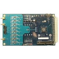
Manufacturer Part Number
EVAL-AD7689EDZ
Description
BOARD EVAL AD7689
Manufacturer
Analog Devices Inc
Series
PulSAR®r
Specifications of EVAL-AD7689EDZ
Number Of Adc's
1
Number Of Bits
16
Sampling Rate (per Second)
250k
Data Interface
Serial
Inputs Per Adc
8 Single Ended
Input Range
±VREF
Power (typ) @ Conditions
12.5mW @ 250kSPS, 5 V
Voltage Supply Source
Single Supply
Operating Temperature
-40°C ~ 85°C
Utilized Ic / Part
AD7689
Silicon Manufacturer
Analog Devices
Application Sub Type
ADC
Kit Application Type
Data Converter
Silicon Core Number
AD7689
Lead Free Status / RoHS Status
Lead free / RoHS Compliant


AD7682/AD7689
DRIVER AMPLIFIER CHOICE
Although the AD7682/AD7689 are easy to drive, the driver
amplifier must meet the following requirements:
•
•
•
Table 9. Recommended Driver Amplifiers
Amplifier
ADA4841-x
AD8655
AD8021
AD8022
OP184
AD8605,
The noise generated by the driver amplifier must be kept as
low as possible to preserve the SNR and transition noise
performance of the AD7682/AD7689. Note that the AD7682/
AD7689 have a noise much lower than most of the other
16-bit ADCs and, therefore, can be driven by a noisier
amplifier to meet a given system noise specification. The
noise from the amplifier is filtered by the AD7682/AD7689
analog input circuit low-pass filter made by R
by an external filter, if one is used. Because the typical noise
of the AD7682/AD7689 is 35 μV rms (with V
SNR degradation due to the amplifier is
where:
f
AD7689 (1.7 MHz in full BW or 425 kHz in ¼ BW) or the
cutoff frequency of an input filter, if one is used.
N is the noise gain of the amplifier (for example, 1 in buffer
configuration).
e
nV/√Hz.
For ac applications, the driver should have a THD perfor-
mance commensurate with the AD7682/AD7689. Figure 18
shows THD vs. frequency for the AD7682/AD7689.
For multichannel, multiplexed applications on each input
or input pair, the driver amplifier and the AD7682/AD7689
analog input circuit must settle a full-scale step onto the
capacitor array at a 16-bit level (0.0015%). In amplifier data
sheets, settling at 0.1% to 0.01% is more commonly
specified. This may differ significantly from the settling
time at a 16-bit level and should be verified prior to driver
selection.
–3dB
N
is the equivalent input noise voltage of the op amp, in
AD8615
is the input bandwidth in megahertz of the AD7682/
SNR
LOSS
=
Typical Application
Very low noise, small, and low power
5 V single supply, low noise
Very low noise and high frequency
Low noise and high frequency
Low power, low noise, and low frequency
5 V single supply, low power
20
log
⎛
⎜
⎜
⎜
⎜ ⎜
⎝
35
2
+
π
2
f
35
−
3dB
(
Ne
N
REF
)
IN
2
and C
= 5 V), the
⎞
⎟
⎟
⎟
⎟ ⎟
⎠
IN
Rev. B | Page 20 of 32
or
VOLTAGE REFERENCE OUTPUT/INPUT
The AD7682/AD7689 allow the choice of a very low temper-
ature drift internal voltage reference, an external reference, or an
external buffered reference.
The internal reference of the AD7682/AD7689 provide excel-
lent performance and can be used in almost all applications.
There are six possible choices of voltage reference schemes
briefly described in Table 10, with more details in each of the
following sections.
Internal Reference/Temperature Sensor
The precision internal reference, suitable for most applications,
can be set for either a 2.5 V or a 4.096 V output, as detailed in
Table 10. With the internal reference enabled, the band gap
voltage is also present on the REFIN pin, which requires an
external 0.1 μF capacitor. Because the current output of REFIN
is limited, it can be used as a source if followed by a suitable
buffer, such as the AD8605. Note that the voltage of REFIN
changes depending on the 2.5 V or 4.096 V internal reference.
Enabling the reference also enables the internal temperature
sensor, which measures the internal temperature of the
AD7682/AD7689 and is thus useful for performing a system
calibration. Note that, when using the temperature sensor, the
output is straight binary referenced from the AD7682/AD7689
GND pin.
The internal reference is temperature-compensated to within
10 mV. The reference is trimmed to provide a typical drift of
±10 ppm/°C.
Connect the AD7682/AD7689 as shown in Figure 31 for either
a 2.5 V or 4.096 V internal reference.
Figure 31. 2.5 V or 4.096 V Internal Reference Connection
10µF
AD7682/
AD7689
REF
TEMP
GND
REFIN
100nF
Related parts for EVAL-AD7689EDZ
Image
Part Number
Description
Manufacturer
Datasheet
Request
R


Part Number:
Description:
BOARD EVAL FOR SI270X-A
Manufacturer:
Silicon Laboratories Inc
Datasheet:

Part Number:
Description:
BUCK CONV REF DESIGN KIT IP1201
Manufacturer:
International Rectifier
Datasheet:
Part Number:
Description:
BOARD DEMO SYNC DUAL BUCK CNVTER
Manufacturer:
International Rectifier
Datasheet:
Part Number:
Description:
BOARD DEMO SYNC BUCK CONVETER
Manufacturer:
International Rectifier
Datasheet:

Part Number:
Description:
EVALBOARD/EB Omnidirectional microphone - Analog
Manufacturer:
Analog Devices
Datasheet:
Part Number:
Description:
EVALBOARD/EB Omnidirectional microphone - Analog
Manufacturer:
Analog Devices
Datasheet:


Part Number:
Description:
BOARD EVAL LED DRIVER LT3756
Manufacturer:
Linear Technology
Datasheet:

Part Number:
Description:
BOARD EVAL FOR AD7741/7742
Manufacturer:
Analog Devices Inc
Datasheet:

Part Number:
Description:
±1.7g Dual-Axis IMEMS Accelerometer Evaluation Board
Manufacturer:
Analog Devices Inc
Datasheet:

Part Number:
Description:
IC MULTIPLIER ANALOG 8-SOIC T/R
Manufacturer:
Analog Devices Inc
Datasheet:

Part Number:
Description:
IC ANALOG MULTIPLIER 8-DIP
Manufacturer:
Analog Devices Inc
Datasheet:
Part Number:
Description:
IC ANALOG MULTIPLIER 8-SOIC
Manufacturer:
Analog Devices Inc
Datasheet:
Part Number:
Description:
IC ANALOG MULTIPLIER 8-DIP
Manufacturer:
Analog Devices Inc
Datasheet: