CDB5376 Cirrus Logic Inc, CDB5376 Datasheet - Page 29
CDB5376
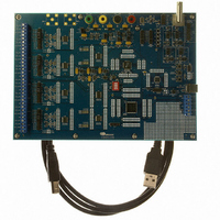
Manufacturer Part Number
CDB5376
Description
EVALUATION BOARD FOR CS5376
Manufacturer
Cirrus Logic Inc
Datasheets
1.CS5371A-ISZR.pdf
(32 pages)
2.CS4373A-ISZ.pdf
(34 pages)
3.CS5376A-IQZR.pdf
(106 pages)
4.CDB5378.pdf
(16 pages)
5.CDB5376.pdf
(80 pages)
6.CDB5376.pdf
(16 pages)
Specifications of CDB5376
Main Purpose
Seismic Evaluation System
Embedded
Yes, MCU, 8-Bit
Utilized Ic / Part
CS3301A, CS3302A, CS4373A, CS5372A, CS5376A
Primary Attributes
Quad Digital Filter
Secondary Attributes
Graphical User Interface, SPI™ & USB Interfaces
Processor To Be Evaluated
CS330x, CS4373A, CS537x
Interface Type
USB
Lead Free Status / RoHS Status
Contains lead / RoHS non-compliant
Lead Free Status / RoHS Status
Lead free / RoHS Compliant, Contains lead / RoHS non-compliant
Other names
598-1778


rejected
Power Supply Characteristics
9.4 SCR Latch-up
The VA- pin is tied to the CS4373A CMOS
substrate and must always be the most-nega-
tive voltage applied to the device to ensure
SCR latch-up does not occur. In general,
latch-up may occur when any pin voltage ex-
ceeds
Absolute Maximum Ratings
It is recommended to connect the VA- power
supply to system ground (GND) with a re-
verse-biased Schottky diode. At power up, if
the VA+ power supply ramps before the VA-
supply is established, the VA- pin voltage
could be pulled above ground potential
through the CS4373A device. If the VA- supply
is pulled 0.7 V or more above GND, SCR
latch-up can occur. A reverse-biased Schottky
diode will clamp the VA- voltage a maximum of
0.3 V above ground to ensure SCR latch-up
does not occur at power up.
9.5 DC-DC Converters
Many low-frequency measurement systems
DS699F2
the
as
specified
limits
table.
table.
of
in
the
the
are battery powered and utilize DC-DC con-
verters to efficiently generate power supply
voltages. To minimize interference effects, op-
erate the DC-DC converter at a frequency
which is rejected by the digital filter, or operate
it synchronous to the MCLK rate.
A synchronous DC-DC converter whose oper-
ating frequency is derived from MCLK will the-
oretically minimize the potential for “beat
frequencies” to appear in the measurement
bandwidth. However this requires the source
clock to remain jitter-free within the DC-DC
converter circuitry. If clock jitter can occur with-
in the DC-DC converter (as in a PLL-based ar-
chitecture),
synchronous DC-DC converter whose switch-
ing frequency is rejected by the digital filter.
During PCB layout, do not place high-current
DC-DC converters near sensitive analog com-
ponents. Carefully routing a separate DC-DC
“star” ground will help isolate noisy switching
currents away from the sensitive analog com-
ponents.
it’s
better
to
use
CS4373A
a
non-
29
Related parts for CDB5376
Image
Part Number
Description
Manufacturer
Datasheet
Request
R

Part Number:
Description:
Development Kit
Manufacturer:
Cirrus Logic Inc
Datasheet:
Part Number:
Description:
Development Kit
Manufacturer:
Cirrus Logic Inc
Datasheet:


Part Number:
Description:
High-efficiency PFC + Fluorescent Lamp Driver Reference Design
Manufacturer:
Cirrus Logic Inc
Datasheet:
Part Number:
Description:
Development Kit
Manufacturer:
Cirrus Logic Inc
Datasheet:
Part Number:
Description:
Development Kit
Manufacturer:
Cirrus Logic Inc
Datasheet:

Part Number:
Description:
Development Kit
Manufacturer:
Cirrus Logic Inc
Datasheet:
Part Number:
Description:
Development Kit
Manufacturer:
Cirrus Logic Inc
Datasheet:
Part Number:
Description:
Development Kit
Manufacturer:
Cirrus Logic Inc
Datasheet:
Part Number:
Description:
Development Kit
Manufacturer:
Cirrus Logic Inc
Datasheet:

Part Number:
Description:
EVALUATION BOARD FOR CS8427
Manufacturer:
Cirrus Logic Inc
Datasheet:

Part Number:
Description:
BOARD EVAL FOR CS8416 RCVR
Manufacturer:
Cirrus Logic Inc
Datasheet:

Part Number:
Description:
EVALUATION BOARD FOR CS8420
Manufacturer:
Cirrus Logic Inc
Datasheet:

Part Number:
Description:
KIT DEVELOPMENT EP9315 ARM9
Manufacturer:
Cirrus Logic Inc
Datasheet:

Part Number:
Description:
KIT DEVELOPMENT EP9302 ARM9
Manufacturer:
Cirrus Logic Inc
Datasheet: