CDB5376 Cirrus Logic Inc, CDB5376 Datasheet - Page 25
CDB5376
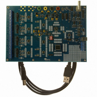
Manufacturer Part Number
CDB5376
Description
EVALUATION BOARD FOR CS5376
Manufacturer
Cirrus Logic Inc
Datasheets
1.CS5371A-ISZR.pdf
(32 pages)
2.CS4373A-ISZ.pdf
(34 pages)
3.CS5376A-IQZR.pdf
(106 pages)
4.CDB5378.pdf
(16 pages)
5.CDB5376.pdf
(80 pages)
6.CDB5376.pdf
(16 pages)
Specifications of CDB5376
Main Purpose
Seismic Evaluation System
Embedded
Yes, MCU, 8-Bit
Utilized Ic / Part
CS3301A, CS3302A, CS4373A, CS5372A, CS5376A
Primary Attributes
Quad Digital Filter
Secondary Attributes
Graphical User Interface, SPI™ & USB Interfaces
Processor To Be Evaluated
CS330x, CS4373A, CS537x
Interface Type
USB
Lead Free Status / RoHS Status
Contains lead / RoHS non-compliant
Lead Free Status / RoHS Status
Lead free / RoHS Compliant, Contains lead / RoHS non-compliant
Other names
598-1778


When enabled, attenuation is applied to both
the OUT and BUF differential analog outputs.
The OUT± pins connect directly into the inter-
nal attenuator resistors and so attenuation ac-
curacy is highly sensitive to load impedance
on the OUT± pins. Loading on the BUF± pins
does not affect attenuator accuracy.
The attenuation settings of CS4373A match
the gain ranges of the CS3301A / CS3302A
differential amplifiers to enable full-scale test-
ing
CS3301A / CS3302A amplifier gain settings
(GAIN) are decoded identical to the CS4373A
attenuator settings (ATT) and so can share
GPIO signals from the digital filter.
7.3 OUT± Precision Output
The OUT± pins are precision differential ana-
log outputs for testing the high-performance
electronics measurement channel. These pre-
cision outputs have higher performance spec-
ifications than the BUF outputs, but with a
much higher sensitivity to external loading. Ex-
cessive resistive or capacitive loading on the
OUT± pins will degrade the analog perfor-
mance characteristics of the CS4373A in all
operational modes.
The OUT± precision output is optimized for di-
rect connection to the CS3301A / CS3302A
amplifier differential inputs, which have very
high input impedance. These amplifiers in-
clude a pin-controlled input multiplexer to
switch between an internal differential termina-
tion for noise tests and two external differential
inputs. One external amplifier input is typically
dedicated to sensor measurements and the
other to testing the electronics channel.
The OUT± outputs are enabled in all opera-
tional modes except “AC BUF Only” mode
(MODE 3) and sleep modes (MODE 0, 7). In
DS699F2
at
all
gain
ranges.
The
AC BUF Only and sleep modes the OUT± pins
are high impedance.
7.4 BUF± Buffered Output
The BUF± pins are buffered differential analog
outputs for testing external sensors such as
geophones or hydrophones. The buffered out-
puts have reduced performance specifications
compared with the OUT outputs, but are less
sensitive to external loading.
The BUF± outputs are enabled in all operation-
al
(MODE 2) and sleep modes (MODE 0, 7). In
AC OUT Only and sleep modes the BUF± pins
are high impedance to ensure they do not in-
terfere with sensor operation during normal
data acquisition.
For sensor impedance testing, it is required to
place matched series resistors in between the
BUF± outputs and the differential sensor. With
known series resistors and a known DC differ-
ential source voltage, sensor resistance can
be calculated ratiometrically from the mea-
sured voltage drop across the sensor.
7.5 CAP± Analog Output
The CS4373A requires a 10 nF C0G or NPO-
type capacitor connected differentially across
the CAP± pins. This capacitor creates an inter-
nal anti-alias filter to eliminate high-frequency
signals from the OUT± and BUF± analog out-
puts and helps to maintain the stability of the
low-power ∆Σ circuitry.
A COG, NPO or similar high-quality capacitor
is required for CAP
types, such as X7R, do not have the required
linearity. Using a poor-quality capacitor on
CAP± will significantly degrade THD perfor-
mance in the AC operational modes.
modes
except
±
“AC OUT Only”
since other capacitor
CS4373A
mode
25
Related parts for CDB5376
Image
Part Number
Description
Manufacturer
Datasheet
Request
R

Part Number:
Description:
Development Kit
Manufacturer:
Cirrus Logic Inc
Datasheet:
Part Number:
Description:
Development Kit
Manufacturer:
Cirrus Logic Inc
Datasheet:


Part Number:
Description:
High-efficiency PFC + Fluorescent Lamp Driver Reference Design
Manufacturer:
Cirrus Logic Inc
Datasheet:
Part Number:
Description:
Development Kit
Manufacturer:
Cirrus Logic Inc
Datasheet:
Part Number:
Description:
Development Kit
Manufacturer:
Cirrus Logic Inc
Datasheet:

Part Number:
Description:
Development Kit
Manufacturer:
Cirrus Logic Inc
Datasheet:
Part Number:
Description:
Development Kit
Manufacturer:
Cirrus Logic Inc
Datasheet:
Part Number:
Description:
Development Kit
Manufacturer:
Cirrus Logic Inc
Datasheet:
Part Number:
Description:
Development Kit
Manufacturer:
Cirrus Logic Inc
Datasheet:

Part Number:
Description:
EVALUATION BOARD FOR CS8427
Manufacturer:
Cirrus Logic Inc
Datasheet:

Part Number:
Description:
BOARD EVAL FOR CS8416 RCVR
Manufacturer:
Cirrus Logic Inc
Datasheet:

Part Number:
Description:
EVALUATION BOARD FOR CS8420
Manufacturer:
Cirrus Logic Inc
Datasheet:

Part Number:
Description:
KIT DEVELOPMENT EP9315 ARM9
Manufacturer:
Cirrus Logic Inc
Datasheet:

Part Number:
Description:
KIT DEVELOPMENT EP9302 ARM9
Manufacturer:
Cirrus Logic Inc
Datasheet: