CDB5376 Cirrus Logic Inc, CDB5376 Datasheet - Page 22
CDB5376
Manufacturer Part Number
CDB5376
Description
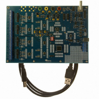
EVALUATION BOARD FOR CS5376
Manufacturer
Cirrus Logic Inc
Datasheets
1.CS5371A-ISZR.pdf
(32 pages)
2.CS4373A-ISZ.pdf
(34 pages)
3.CS5376A-IQZR.pdf
(106 pages)
4.CDB5378.pdf
(16 pages)
5.CDB5376.pdf
(80 pages)
6.CDB5376.pdf
(16 pages)
Specifications of CDB5376
Main Purpose
Seismic Evaluation System
Embedded
Yes, MCU, 8-Bit
Utilized Ic / Part
CS3301A, CS3302A, CS4373A, CS5372A, CS5376A
Primary Attributes
Quad Digital Filter
Secondary Attributes
Graphical User Interface, SPI™ & USB Interfaces
Processor To Be Evaluated
CS330x, CS4373A, CS537x
Interface Type
USB
Lead Free Status / RoHS Status
Contains lead / RoHS non-compliant
Lead Free Status / RoHS Status
Lead free / RoHS Compliant, Contains lead / RoHS non-compliant
Other names
598-1778


6. DIGITAL INPUTS
The CS4373A is designed to operate with the
CS5376A digital filter. The digital filter gener-
ates one-bit ∆Σ test bit stream data (TDATA),
a master clock (MCLK) and a synchronization
signal (MSYNC). In addition, the digital filter
GPIO pins control the CS4373A operational
mode (MODE) and attenuator (ATT) settings.
6.1 TDATA Connection
The TDATA digital input expects encoded
one-bit ∆Σ data nominally at a 256 kHz rate.
The one’s density input range is approximately
25% minimum to 75% maximum, with differen-
tial mid-scale at 50% one’s density.
The CS5376A digital filter test bit stream
(TBS) generator can encode two types of AC
signals as over-sampled, one-bit ∆Σ data - a
pure sine wave for THD and CMRR testing or
a triggerable impulse waveform for synchroni-
zation testing and impulse response charac-
terization. In the AC operational modes, the
CS4373A converts the over-sampled bit
stream digital data into precision differential or
common mode analog AC signals.
The CS5376A TBS sine mode encodes an ap-
proximately 5 V
with a digital filter TBSGAIN register setting of
0x04B8F2. Because TBS impulse mode en-
codes frequencies above 100 Hz, a maximum
0x0078E5 TBSGAIN impulse mode register
setting is specified to guarantee stability of the
22
pp
full-scale sine wave signal
SENSOR
ELECTRONICS
CH1 BUF
CH1,2,3,4 OUT
CH2 BUF
VA+
CH3 BUF
VA-
CH4 BUF
VREF
2.5 V
Switches
CONTROL
Analog
SWITCH
Figure 11. Digital Inputs
10 Ω
100µF
+
Route VREF as diff pair
Route OUT as diff pair
Route BUF as diff pair
VA+
VA-
10nF
C0G
CS4373A low-power ∆Σ circuitry. Details on
the setup and operation of the digital filter TBS
generator can be found in the CS5376A data
sheet.
6.2 MCLK Connection
The CS5376A digital filter generates the mas-
ter clock for CS4373A, typically 2.048 MHz,
from a synchronous CLK input from the exter-
nal system. By default, MCLK is disabled at re-
set and is enabled by writing the digital filter
CONFIG register. If MCLK is disabled during
operation, the CS4373A will enter power down
after approximately 40
MCLK must have low in-band jitter to guaran-
tee full analog performance, requiring a crys-
tal- or VCXO-based system clock into the
digital filter. Clock jitter on the digital filter ex-
ternal CLK input directly translates to jitter on
MCLK.
6.3 MSYNC Connection
The CS5376A digital filter also provides a syn-
chronization signal to the CS4373A. The
MSYNC signal is generated following a rising
edge received on the digital filter SYNC input.
By default MSYNC generation is disabled at
reset and is enabled by writing to the digital fil-
ter CONFIG register.
The input SYNC signal to the CS5376A digital
filter sets a common reference time t
0.1µF
0.1µF
CAP+
CAP-
BUF+
BUF-
OUT+
OUT-
VREF+
VREF-
VA-
VA-
CS4373A
DGND
MSYNC
MODE0
MODE1
MODE2
VD
TDATA
MCLK
ATT0
ATT1
ATT2
0.1µF
MCLK
MSYNC
TBSDATA
GPIO
GPIO
GPIO
GPIO
GPIO
GPIO
CS5376A
SIGNALS
VD
µ
S.
CS4373A
0
for mea-
DS699F2
Related parts for CDB5376
Image
Part Number
Description
Manufacturer
Datasheet
Request
R

Part Number:
Description:
Development Kit
Manufacturer:
Cirrus Logic Inc
Datasheet:
Part Number:
Description:
Development Kit
Manufacturer:
Cirrus Logic Inc
Datasheet:


Part Number:
Description:
High-efficiency PFC + Fluorescent Lamp Driver Reference Design
Manufacturer:
Cirrus Logic Inc
Datasheet:
Part Number:
Description:
Development Kit
Manufacturer:
Cirrus Logic Inc
Datasheet:
Part Number:
Description:
Development Kit
Manufacturer:
Cirrus Logic Inc
Datasheet:

Part Number:
Description:
Development Kit
Manufacturer:
Cirrus Logic Inc
Datasheet:
Part Number:
Description:
Development Kit
Manufacturer:
Cirrus Logic Inc
Datasheet:
Part Number:
Description:
Development Kit
Manufacturer:
Cirrus Logic Inc
Datasheet:
Part Number:
Description:
Development Kit
Manufacturer:
Cirrus Logic Inc
Datasheet:

Part Number:
Description:
EVALUATION BOARD FOR CS8427
Manufacturer:
Cirrus Logic Inc
Datasheet:

Part Number:
Description:
BOARD EVAL FOR CS8416 RCVR
Manufacturer:
Cirrus Logic Inc
Datasheet:

Part Number:
Description:
EVALUATION BOARD FOR CS8420
Manufacturer:
Cirrus Logic Inc
Datasheet:

Part Number:
Description:
KIT DEVELOPMENT EP9315 ARM9
Manufacturer:
Cirrus Logic Inc
Datasheet:

Part Number:
Description:
KIT DEVELOPMENT EP9302 ARM9
Manufacturer:
Cirrus Logic Inc
Datasheet: