CDB5376 Cirrus Logic Inc, CDB5376 Datasheet
CDB5376
Specifications of CDB5376


Related parts for CDB5376


CDB5376 Summary of contents
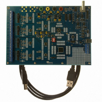
Page 1
High-Z, Programmable Gain, Differential Amplifier Features & Description Signal Bandwidth kHz Selectable Gain: x1, x2, x4, x8, x16, x32, x64 Differential Inputs, Differential Outputs • Multiplexed inputs: INA, INB, 800Ω termination • Rough / fine charge outputs ...
Page 2
TABLE OF CONTENTS 1. CHARACTERISTICS AND SPECIFICATIONS ....................................................................... 4 SPECIFIED OPERATING CONDITIONS ................................................................................ 4 ABSOLUTE MAXIMUM RATINGS .......................................................................................... 4 THERMAL CHARACTERISTICS ............................................................................................. 5 ANALOG CHARACTERISTICS ............................................................................................... 5 DIGITAL CHARACTERISTICS ................................................................................................ 8 POWER SUPPLY CHARACTERISTICS ................................................................................. 9 2. GENERAL DESCRIPTION..................................................................................................... 10 ...
Page 3
REVISION HISTORY Revision Date PP1 NOV 2007 Contacting Cirrus Logic Support For all product questions and inquiries contact a Cirrus Logic Sales Representative. To find one nearest you go to www.cirrus.com IMPORTANT NOTICE "Preliminary" product information describes products that are ...
Page 4
CHARACTERISTICS AND SPECIFICATIONS • Min/Max characteristics and specifications are guaranteed over the Specified Operating Conditions. • Typical performance characteristics and specifications are derived from measurements taken at nom- inal supply voltages and T A • GND = 0 V, ...
Page 5
THERMAL CHARACTERISTICS Parameter Storage Temperature Range Allowable Junction Temperature Junction to Ambient Thermal Impedance Ambient Operating Temperature ANALOG CHARACTERISTICS Parameter Noise Performance Input Voltage Noise Input Voltage Noise Density Input Current Noise Density Distortion Performance Total Harmonic Distortion (Note 5) ...
Page 6
ANALOG CHARACTERISTICS (CONT.) Parameter Gain Gain, Differential Gain, Common Mode Gain Accuracy, Absolute Gain Accuracy, Relative (Note 8) Gain Drift Offset Offset Voltage, Input Referred Offset After Calibration, Absolute Offset Calibration Range Offset Voltage Drift Notes: 6. Common mode signals ...
Page 7
ANALOG CHARACTERISTIC (Cont.) Parameter Analog Input Characteristics Input Signal Frequencies Input Voltage Range (Signal + Vcm) Full Scale Input, Differential Input Impedance, Differential Input Impedance, Common Mode Input Bias Current Crosstalk, Multiplexed Inputs Common to Differential Mode Rejection Analog Output ...
Page 8
DIGITAL CHARACTERISTICS Parameter Digital Characteristics High-level Input Drive Voltage Low-level Input Drive Voltage Input Leakage Current Digital Input Capacitance Rise Times Fall Times Notes: 15. Device is intended to be driven with CMOS logic levels. Input Selection MUX1 800 Ω ...
Page 9
POWER SUPPLY CHARACTERISTICS Parameter Power Supply Current, Normal Mode Analog Power Supply Current Digital Power Supply Current Power Supply Current, Power Down Mode Analog Power Supply Current, PWDN = 1 Digital Power Supply Current, PWDN = 1 Power Supply Rejection ...
Page 10
GENERAL DESCRIPTION The CS3302A is a high-impedance, low-noise CMOS differential input, differential output ampli- fier for precision analog signals between DC and 2 kHz. It has multiplexed inputs, rough/fine charge outputs, and programmable gains of x1, x2, x4, x8, ...
Page 11
Differential M Sensor U AMP X requires two series resistors and a differential capaci- tor to create the modulator anti-alias RC filter. 2.1.3 Differential Signals Analog signals into and out of the CS3302A are differential, consisting of two halves with ...
Page 12
Mux Selection The analog inputs to the amplifier are multiplexed, with external signals applied to the INA+, INA- or INB+, INB- pins. An internal termination is also available for noise tests. Input mux selection is made using the MUX0 ...
Page 13
Connection Diagram shows a connection diagram for the CS3302A amplifier when used with the CS5372A dual ∆Σ Figure 5 modulator, the CS4373A test DAC and the CS5376A digital filter. The diagram shows differential sensors, a test DAC, and analog ...
Page 14
PIN DESCRIPTION Pin Name Pin # I/O VA Positive analog supply voltage. VA Negative analog supply voltage Positive digital supply voltage. GND 15 Ground. INA+, INA Channel ...
Page 15
ORDERING INFORMATION Model CS3302A-IS CS3302A-ISZ, lead (Pb) free 5. ENVIRONMENTAL, MANUFACTURING, & HANDLING INFORMATION Model Number CS3302A-IS CS3302A-ISZ, lead (Pb) free * MSL (Moisture Sensitivity Level) as specified by IPC/JEDEC J-STD-020. DS765PP1 CS3302A DS765PP1 Temperature -40 to +85 °C ...
Page 16
PACKAGE DIMENSIONS 24 PIN SSOP PACKAGE DRAWING TOP VIEW DIM ∝ Notes: 1. “D” and “E1” are reference datums and do not included mold flash ...