DC-VIDEO-TVP5146N Altera, DC-VIDEO-TVP5146N Datasheet - Page 9
DC-VIDEO-TVP5146N
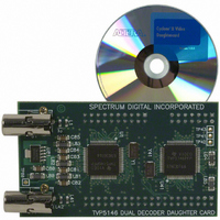
Manufacturer Part Number
DC-VIDEO-TVP5146N
Description
VIDEO DAUGHTER CARD
Manufacturer
Altera
Series
Stratix® IIIr
Datasheets
1.EP3SL150F780C4N.pdf
(16 pages)
2.EP3SL150F780C4N.pdf
(332 pages)
3.DC-VIDEO-TVP5146N.pdf
(58 pages)
Specifications of DC-VIDEO-TVP5146N
Main Purpose
Video, Daughter Card
Embedded
No
Utilized Ic / Part
Altera Dev Kits
Primary Attributes
Dual Composite Video Input - NTSC or PAL
Secondary Attributes
10-bit BT.656 Output, Compatible with Expansion Connector, Standard on Most Altera Development Kits
Lead Free Status / RoHS Status
Lead free / RoHS Compliant
Other names
544-1704


Chapter 1: Stratix III Device Datasheet: DC and Switching Characteristics
Electrical Characteristics
Table 1–13. Single-Ended I/O Standards Specifications
© July 2010 Altera Corporation
3.3-V LVTTL
3.0-V LVTTL
3.3-V LVCMOS
3.0-V LVCMOS
2.5-V LVTTL/
LVCMOS
1.8-V LVTTL /
LVCMOS
1.5-V LVTTL/
LVCMOS
1.2-V LVTTL /
LVCMOS
3.0-V PCI
3.0-V PCI-X
I/O Standard
3.135
3.135
2.375
1.425
Min
2.85
2.85
1.71
1.14
2.85
2.85
V
Internal Weak Pull-Up Resistor
Table 1–12
Table 1–12. Internal Weak Pull-Up Resistor for Stratix III Devices
I/O Standard Specifications
The following tables list input voltage sensitivities (V
(V
supported by Stratix III devices. V
I
Table 1–13
specifications. Refer to
the
CCIO
OL
R
Notes to
(1) All I/O pins have an option to enable weak pull-up except configuration, test, and JTAG pins.
(2) Pin pull-up resistance values may be lower if an external source drives the pin higher than V
(3) The internal weak pull-down feature is only available for the JTAG TCK pin. The typical value for this internal weak
Typ
3.3
3.3
2.5
2.5
2.5
1.8
1.5
1.2
Symbol
PU
3
3
3
3
OH
and I
(V)
Table 1–14
pull-down resistor is approximately 25k .
and V
3.465
3.465
2.625
2.625
2.625
1.575
Max Min
3.15
3.15
1.89
1.26
3.15
3.15
Table
OH
, respectively.
Value of the I/O pin pull-
up resistor before and
during configuration, as
well as user mode if the
programmable pull-up
resistor option is
enabled
lists the weak pull-up resistor values for Stratix III devices.
OL
through
1–12:
), and current drive characteristics (I
-0.3
-0.3
-0.3
-0.3
-0.3
-0.3
-0.3
-0.3
-0.3
-0.3
—
—
through
Parameter
V
0.35 * V
0.35 * V
0.35 * V
0.35 * V
IL
0.3 * V
Table 1–18
(V)
Max
0.8
0.8
0.8
0.8
0.7
0.7
0.7
“Glossary” on page 1–326
Table
CCIO
CCIO
CCIO
CCIO
CCIO
1–18.
0.65 * V
0.65 * V
0.65 * V
0.5 * V
0.5 * V
list the Stratix III device family I/O standard
Min
1.7
1.7
1.7
1.7
1.7
1.7
1.7
V
V
V
V
V
V
OL
CCIO
CCIO
CCIO
CCIO
CCIO
CCIO
CCIO
CCIO
CCIO
CCIO
CCIO
and V
= 3.3 V ± 5%
= 1.8 V ± 5%
V
= 3.0 V ± 5%
= 2.5 V ± 5%
= 1.5 V ± 5%
= 1.2 V ± 5%
IH
Conditions
(V)
V
V
V
CCIO
CCIO
CCIO
OH
Max
3.6
3.6
3.6
3.6
3.6
3.6
3.6
3.6
—
+ 0.3
+ 0.3
+ 0.3
values are valid at the corresponding
(2)
(2)
(2)
(2)
(2)
(2)
OH
for an explanation of terms used in
0.25 * V
0.25 * V
and I
0.1 * V
0.1 * V
V
IH
Max
0.45
OL
0.4
0.4
0.2
0.2
0.2
0.4
0.7
and V
(V)
(Note
OL
Min
CCIO
CCIO
—
—
—
—
—
—
CCIO
CCIO
Stratix III Device Handbook, Volume 2
) for all I/O standards
IL
1),
0.75 * V
0.75 * V
), output voltages
V
0.9 * V
0.9 * V
V
V
CCIO
V
CCIO
CCIO
(3)
Typ
Min
OH
25
25
25
25
25
25
2.4
2.4
2.1
1.7
2
- 0.45
- 0.2
- 0.2
(V)
CCIO
CCIO
CCIO
CCIO
CCIO
Max
.
—
—
—
—
—
—
(mA)
IOL
0.1
0.1
0.1
1.5
1.5
2
2
1
2
2
2
2
Unit
(mA)
k
k
k
k
k
k
IOH
-0.1
-0.1
-0.1
-0.5
-0.5
-2
-2
-1
-2
-2
-2
-2
1–9
Related parts for DC-VIDEO-TVP5146N
Image
Part Number
Description
Manufacturer
Datasheet
Request
R

Part Number:
Description:
CYCLONE II STARTER KIT EP2C20N
Manufacturer:
Altera
Datasheet:


Part Number:
Description:
CPLD, EP610 Family, ECMOS Process, 300 Gates, 16 Macro Cells, 16 Reg., 16 User I/Os, 5V Supply, 35 Speed Grade, 24DIP
Manufacturer:
Altera Corporation
Datasheet:
Part Number:
Description:
CPLD, EP610 Family, ECMOS Process, 300 Gates, 16 Macro Cells, 16 Reg., 16 User I/Os, 5V Supply, 15 Speed Grade, 24DIP
Manufacturer:
Altera Corporation
Datasheet:
Part Number:
Description:
Manufacturer:
Altera Corporation
Datasheet:
Part Number:
Description:
CPLD, EP610 Family, ECMOS Process, 300 Gates, 16 Macro Cells, 16 Reg., 16 User I/Os, 5V Supply, 30 Speed Grade, 24DIP
Manufacturer:
Altera Corporation
Datasheet:
Part Number:
Description:
High-performance, low-power erasable programmable logic devices with 8 macrocells, 10ns
Manufacturer:
Altera Corporation
Datasheet:
Part Number:
Description:
High-performance, low-power erasable programmable logic devices with 8 macrocells, 7ns
Manufacturer:
Altera Corporation
Datasheet:
Part Number:
Description:
Classic EPLD
Manufacturer:
Altera Corporation
Datasheet:
Part Number:
Description:
High-performance, low-power erasable programmable logic devices with 8 macrocells, 10ns
Manufacturer:
Altera Corporation
Datasheet:
Part Number:
Description:
Manufacturer:
Altera Corporation
Datasheet:
Part Number:
Description:
Manufacturer:
Altera Corporation
Datasheet:
Part Number:
Description:
Manufacturer:
Altera Corporation
Datasheet:
Part Number:
Description:
CPLD, EP610 Family, ECMOS Process, 300 Gates, 16 Macro Cells, 16 Reg., 16 User I/Os, 5V Supply, 25 Speed Grade, 24DIP
Manufacturer:
Altera Corporation
Datasheet: