DC-VIDEO-TVP5146N Altera, DC-VIDEO-TVP5146N Datasheet - Page 33
DC-VIDEO-TVP5146N
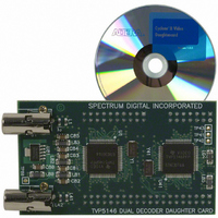
Manufacturer Part Number
DC-VIDEO-TVP5146N
Description
VIDEO DAUGHTER CARD
Manufacturer
Altera
Series
Stratix® IIIr
Datasheets
1.EP3SL150F780C4N.pdf
(16 pages)
2.EP3SL150F780C4N.pdf
(332 pages)
3.DC-VIDEO-TVP5146N.pdf
(58 pages)
Specifications of DC-VIDEO-TVP5146N
Main Purpose
Video, Daughter Card
Embedded
No
Utilized Ic / Part
Altera Dev Kits
Primary Attributes
Dual Composite Video Input - NTSC or PAL
Secondary Attributes
10-bit BT.656 Output, Compatible with Expansion Connector, Standard on Most Altera Development Kits
Lead Free Status / RoHS Status
Lead free / RoHS Compliant
Other names
544-1704


Chapter 1: Stratix III Device Datasheet: DC and Switching Characteristics
I/O Timing
© July 2010 Altera Corporation
5. Compare the results of steps 2 and 4. The increase or decrease in delay must be
The Quartus II software reports the timing with the conditions listed in
using
the output timing of the Quartus II software.
Figure 1–6. Output Delay Timing Report Setup for Single-Ended Outputs and Dedicated Differential
Outputs
Note to
(1) Output pin timing is reported at the output pin of the FPGA device. Additional delays for loading and board trace delay
Figure 1–7
the Quartus II software for differential outputs with single and multiple external
resistors, respectively.
Figure 1–7. Output Delay Timing Report Setup for Differential Outputs with Single External Resistor
Figure 1–8. Output Delay Timing Report Setup for Differential Outputs with Three External Resistor
added to or subtracted from the I/O Standard Output Adder delays to yield the
actual worst-case propagation delay (clock-to-output) of the PCB trace.
must be accounted for with IBIS model simulations.
Figure
Equation 1–1 on page
(Note 1)
and
1–6:
Figure 1–8
Output
Buffer
V
GND
CCIO
Output
show the circuit that is represented by the output timing of
Differential Outputs
Differential Outputs
Non-Dedicated
Non-Dedicated
1–7.
V
MEAS
Figure 1–6
R
S
V
V
V
V
V
GND
MEAS
MEAS
MEAS
MEAS
TT
R
C
shows the circuit that is represented by
T
L
R
R
S
S
R
R
P
P
R
R
D
Stratix III Device Handbook, Volume 2
D
Output
Output
p
n
R
D
Table 1–37
1–33
Related parts for DC-VIDEO-TVP5146N
Image
Part Number
Description
Manufacturer
Datasheet
Request
R

Part Number:
Description:
CYCLONE II STARTER KIT EP2C20N
Manufacturer:
Altera
Datasheet:


Part Number:
Description:
CPLD, EP610 Family, ECMOS Process, 300 Gates, 16 Macro Cells, 16 Reg., 16 User I/Os, 5V Supply, 35 Speed Grade, 24DIP
Manufacturer:
Altera Corporation
Datasheet:
Part Number:
Description:
CPLD, EP610 Family, ECMOS Process, 300 Gates, 16 Macro Cells, 16 Reg., 16 User I/Os, 5V Supply, 15 Speed Grade, 24DIP
Manufacturer:
Altera Corporation
Datasheet:
Part Number:
Description:
Manufacturer:
Altera Corporation
Datasheet:
Part Number:
Description:
CPLD, EP610 Family, ECMOS Process, 300 Gates, 16 Macro Cells, 16 Reg., 16 User I/Os, 5V Supply, 30 Speed Grade, 24DIP
Manufacturer:
Altera Corporation
Datasheet:
Part Number:
Description:
High-performance, low-power erasable programmable logic devices with 8 macrocells, 10ns
Manufacturer:
Altera Corporation
Datasheet:
Part Number:
Description:
High-performance, low-power erasable programmable logic devices with 8 macrocells, 7ns
Manufacturer:
Altera Corporation
Datasheet:
Part Number:
Description:
Classic EPLD
Manufacturer:
Altera Corporation
Datasheet:
Part Number:
Description:
High-performance, low-power erasable programmable logic devices with 8 macrocells, 10ns
Manufacturer:
Altera Corporation
Datasheet:
Part Number:
Description:
Manufacturer:
Altera Corporation
Datasheet:
Part Number:
Description:
Manufacturer:
Altera Corporation
Datasheet:
Part Number:
Description:
Manufacturer:
Altera Corporation
Datasheet:
Part Number:
Description:
CPLD, EP610 Family, ECMOS Process, 300 Gates, 16 Macro Cells, 16 Reg., 16 User I/Os, 5V Supply, 25 Speed Grade, 24DIP
Manufacturer:
Altera Corporation
Datasheet: