DC-VIDEO-TVP5146N Altera, DC-VIDEO-TVP5146N Datasheet - Page 12
DC-VIDEO-TVP5146N
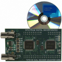
Manufacturer Part Number
DC-VIDEO-TVP5146N
Description
VIDEO DAUGHTER CARD
Manufacturer
Altera
Series
Stratix® IIIr
Datasheets
1.EP3SL150F780C4N.pdf
(16 pages)
2.EP3SL150F780C4N.pdf
(332 pages)
3.DC-VIDEO-TVP5146N.pdf
(58 pages)
Specifications of DC-VIDEO-TVP5146N
Main Purpose
Video, Daughter Card
Embedded
No
Utilized Ic / Part
Altera Dev Kits
Primary Attributes
Dual Composite Video Input - NTSC or PAL
Secondary Attributes
10-bit BT.656 Output, Compatible with Expansion Connector, Standard on Most Altera Development Kits
Lead Free Status / RoHS Status
Lead free / RoHS Compliant
Other names
544-1704


1–12
Table 1–18. Differential I/O Standard Specifications (Part 2 of 2)
Power Consumption
Stratix III Device Handbook, Volume 2
2.5 V LVDS
(Column I/O)
RSDS
(Row I/O)
RSDS
(Column I/O)
Mini-LVDS
(Row I/O)
Mini-LVDS
(Column I/0)
LVPECL
(3)
Notes to
(1) The minimum V
(2) RL range: 90 RL 110 .
(3) Column and row I/O banks support LVPECL I/O standards for input operation only on dedicated clock input pins. Differential clock inputs in column I/O use
(4) The receiver voltage input range for the data rate when D
(5) Power supply for the column I/O LVPECL differential clock input buffer is V
(6) The receiver voltage input range for the data rate when D
Standard
V
The receiver voltage input range for the data rate when D
The receiver voltage input range for the data rate when D
I/O
CC_CLKIN
Table
that must be powered by 2.5 V. Differential clock inputs in row I/O banks are powered by V
f
1–18:
2.375
2.375
2.375
2.375
2.375
2.375
2.375
2.375
Min
(5)
(5)
ID
value is applicable over the entire common mode range, V
V
CCIO
Typ
2.5
2.5
2.5
2.5
2.5
2.5
2.5
2.5
(5)
(5)
Altera offers two ways to estimate power for a design: the Excel-based Early Power
Estimator (EPE) and the Quartus
The interactive Excel-based Early Power Estimator is typically used prior to designing
the FPGA in order to get a magnitude estimate of the device power. The Quartus II
PowerPlay Power Analyzer provides estimation based on the specifics of the design
after place-and-route is complete. The PowerPlay Power Analyzer can apply a
combination of user-entered, simulation-derived, and estimated signal activities
which, when combined with detailed circuit models, can yield very accurate power
estimation.
Refer to
Use the EPE and PowerPlay Power Analyzer for current estimates of remaining
power supplies.
For more information about power estimation tools, refer to the
Estimator User Guide For Stratix III FPGAs
the Quartus II Handbook.
(V)
2.625
2.625
2.625
2.625
2.625
2.625
2.625
2.625
Max
(5)
(5)
Table 1–4 on page 1–5
Min
0.1
0.1
0.1
0.1
0.2
0.2
0.3
0.3
Condition
V
V
V
V
V
CM
CM
CM
CM
ID
= 1.25
= 1.25
= 1.25
= 1.25
—
—
—
—
(V)
(1)
max
max
max
max
> 700 Mbps is 0.85 V V
700 Mbps is 0.45 V V
> 700 Mbps is 1.0 V V
700 Mbps is zero V V
Max
0.6
0.6
—
—
—
—
—
—
Chapter 1: Stratix III Device Datasheet: DC and Switching Characteristics
for supply current estimates for V
II PowerPlay Power Analyzer feature.
0.05
Min
1.05
0.3
0.3
0.4
0.4
0.6
1.0
(6)
(6)
CC_CLKIN
CM
.
Condition
and the
D
D
D
D
.
V
max
max
max
max
ICM(DC)
Mbps
Mbps
Mbps
Mbps
IN
700
—
—
—
—
700
> 700
> 700
IN
IN
IN
1.6 V.
1.75 V.
1.85 V.
1.95 V.
(V)
PowerPlay Power Analysis
1.325
1.325
Max
1.55
1.4
1.4
1.8
(4)
1.6
(4)
1.8
(6)
(6)
CCPD
.
0.247
0.247
0.25
0.25
Min
0.1
0.1
—
—
© July 2010 Altera Corporation
PowerPlay Early Power
V
CCPGM
OD
Typ
0.2
0.2
—
—
—
—
—
—
(V)
Electrical Characteristics
and V
(2)
Max
0.6
0.6
0.6
0.6
0.6
0.6
—
—
chapter in
CC_CLKIN
Min
1.0
1.0
0.5
0.5
0.5
0.5
—
—
.
V
OCM
1.25
1.25
Typ
1.2
1.2
1.2
1.2
(V)
—
—
(2)
Max
1.5
1.5
1.4
1.5
1.4
1.5
—
—
Related parts for DC-VIDEO-TVP5146N
Image
Part Number
Description
Manufacturer
Datasheet
Request
R

Part Number:
Description:
CYCLONE II STARTER KIT EP2C20N
Manufacturer:
Altera
Datasheet:


Part Number:
Description:
CPLD, EP610 Family, ECMOS Process, 300 Gates, 16 Macro Cells, 16 Reg., 16 User I/Os, 5V Supply, 35 Speed Grade, 24DIP
Manufacturer:
Altera Corporation
Datasheet:
Part Number:
Description:
CPLD, EP610 Family, ECMOS Process, 300 Gates, 16 Macro Cells, 16 Reg., 16 User I/Os, 5V Supply, 15 Speed Grade, 24DIP
Manufacturer:
Altera Corporation
Datasheet:
Part Number:
Description:
Manufacturer:
Altera Corporation
Datasheet:
Part Number:
Description:
CPLD, EP610 Family, ECMOS Process, 300 Gates, 16 Macro Cells, 16 Reg., 16 User I/Os, 5V Supply, 30 Speed Grade, 24DIP
Manufacturer:
Altera Corporation
Datasheet:
Part Number:
Description:
High-performance, low-power erasable programmable logic devices with 8 macrocells, 10ns
Manufacturer:
Altera Corporation
Datasheet:
Part Number:
Description:
High-performance, low-power erasable programmable logic devices with 8 macrocells, 7ns
Manufacturer:
Altera Corporation
Datasheet:
Part Number:
Description:
Classic EPLD
Manufacturer:
Altera Corporation
Datasheet:
Part Number:
Description:
High-performance, low-power erasable programmable logic devices with 8 macrocells, 10ns
Manufacturer:
Altera Corporation
Datasheet:
Part Number:
Description:
Manufacturer:
Altera Corporation
Datasheet:
Part Number:
Description:
Manufacturer:
Altera Corporation
Datasheet:
Part Number:
Description:
Manufacturer:
Altera Corporation
Datasheet:
Part Number:
Description:
CPLD, EP610 Family, ECMOS Process, 300 Gates, 16 Macro Cells, 16 Reg., 16 User I/Os, 5V Supply, 25 Speed Grade, 24DIP
Manufacturer:
Altera Corporation
Datasheet: